Global high-mix volume high-speed PCBA manufacturer
9:00 -18:00, Mon. - Fri. (GMT+8)
9:00 -12:00, Sat. (GMT+8)
(Except Chinese public holidays)
Global high-mix volume high-speed PCBA manufacturer
9:00 -18:00, Mon. - Fri. (GMT+8)
9:00 -12:00, Sat. (GMT+8)
(Except Chinese public holidays)
HomePage > Blog > Knowledge Base > PCB Panelization Guidelines | What is it and why is it used?
In modern electronics, efficiency is a key factor for success. As technology advances, modern devices are becoming smaller and more complex yet more efficient in meeting EMI/EMC and thermal management requirements. But how can businesses ensure that their product (especially their circuit board panels) can cater to all these demands and ensure that the process stays cost-effective?
The answer to all these problems is PCB panelization! Even though it supports modern electronics manufacturing. PCB panelization provides the knowledge and insights to make electronic production faster, more efficient, and affordable. In the following section, we are going to break down the process as a guideline that will benefit companies that want to manufacture their products efficiently.
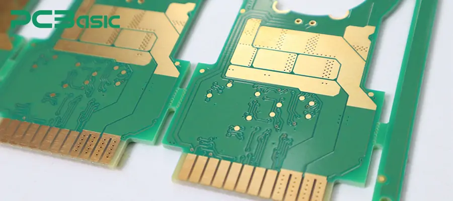
PCB Panelization is a process of electronics manufacturing, where small PCB boards are put together on a single/different array. All the panelized PCBs can later be depanelized and removed from the array as per the product packaging/functionality requirements.
Panelized PCBs can further be depanelized or removed from the array during the installation/packaging phase in the product manufacturing process.
Many benefits come along with the PCB panelization process, but there are many design considerations:
· PCB-array length: with multiple boards on an array, there is a need to improve the strength and reduce vibration during production, which might add more time and complexity during the depanelization phase.
· Layout of components: The layout of the components can add more complexities during PCB panelization. This is especially true for the components/connectors located towards the edge of the PCB.
· PCB structure: The shape of your board might add complications to your PCB panelization process. The best shape for a PCB is a rectangle. In the case of complex PCB boards, using a CAD program will help to put together unusually shaped PCBs into the array.
· Tooling holes: Tooling holes are to be aligned for automated testing on the assembly line and held down during manufacturing.
Those mentioned above are the points that should be considered when taking out panelized PCBs.
Every electronics manufacturing process should incorporate PCB panelization. It helps with mass production, product safety/security, speed and efficiency, etc.
· Improved outcome: Panelized PCBs enhance manufacturing yield by isolating errors to individual boards, minimizing the impact of defects on the overall production process.
· Better quality control: PCB Panelization helps enhance quality control as defects can be identified and traced back to the specific panel. This results in better quality control during the manufacturing process.
· Easy Mounting of Components: PCB panelization helps in making the assembly process easier by using surface-mount technology components.
· Less waste production: Panelized PCB aids in reducing the waste generated during the manufacturing process, as large panels help optimize material usage, and the unused material can then be recycled and reused.
· Improved Efficiency: PCB panel design allows you to add multiple PCB boards to a single panel, reducing the time and cost during the manufacturing process. It also becomes cost-effective while manufacturing boards using the fabricator's processing panels.
Every manufacturer has their preferences for different panel sizes. Generally, the 18X24 inch panels combined with a half-inch perimeter clearance are standard for double-sided boards. However, the ideal PCB panel for a product manufacturing process depends on the requirements of the product.
Here are some different PCB panel combinations:
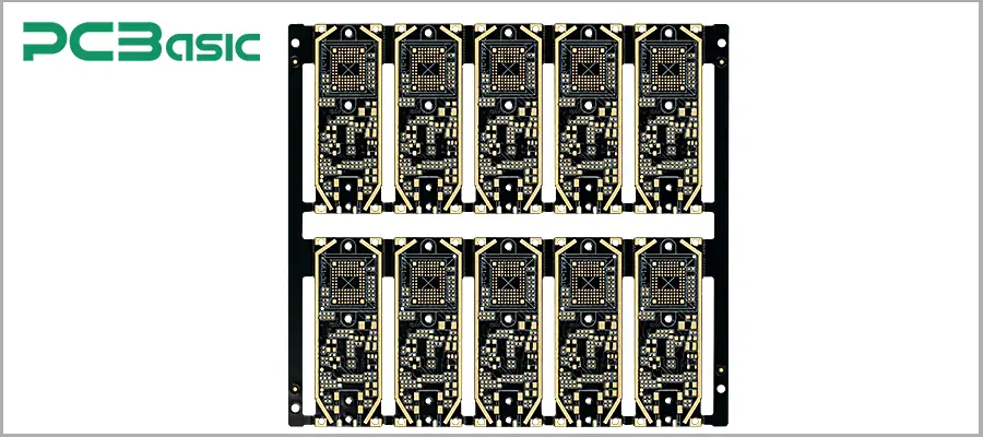
Uniform panelization refers to placing multiple PCBs onto a single panel. This type of PCB combination is frequently used for homogenous PCBs (the PCBs that are similar). Therefore, only one type of PCB is produced on this panel. This is the most popular method as it offers multiple advantages. Firstly, this method of panelization is independent of all the manufacturing conditions or the product portfolio of SMT manufacturers. Secondly, the method is simple and flexible; you can produce more boards while keeping complexities under check.
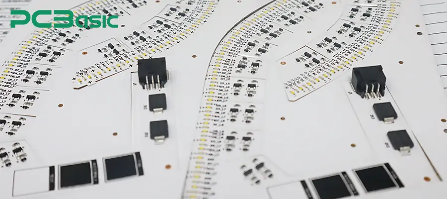
Mixed panelization is a PCB combination where different heterogeneous PCBs are produced simultaneously and connected in a defined ratio depending on the product requirements. It is optional to create a single panel for each type of PCB and a large number of PCBs are not required to be produced during a processing operation.
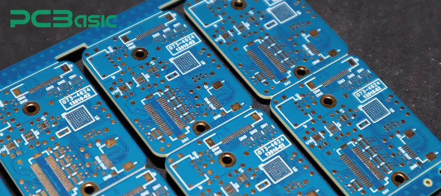
Matrix panelization design is a custom design that uses different PCBs and connects them together based on the manufacturing requirements. Here, the PCB boards are designed for complex operations with a certain functionality depending on the production operation.
Multiple combinations of panelized PCB arrays are used depending on the product requirements. Although it may seem simple, it's not just about grouping boards together for smooth functioning—there are specific PCB panel design guidelines that must be followed.
Consider the size and shape of the PCB panel design, ensuring that they fit the manufacturer's equipment. Fabrication houses might have size limitations, making it essential to optimize the panel layout to fit the required space.
There should be enough edge clearance for the PCB panel edges to ensure proper handling and depanelization. Insufficient edge clearance can lead to misalignment or problems during separation.
Despite the PCB panel design that you choose, there should be design separation considerations, including scoring, tab routing, or mouse bites. Every method has its advantages/disadvantages, depending on the complexity of boards and how precise the separation has to be.
Be sure to consider all the tolerances of your manufacturing processes; it helps to ensure that the PCB panel design is reliable and has minimal chances of defects. By following the above guidelines, you can create an ideal panelized PCB design for the production process with fewer errors and a smooth manufacturing experience.
PCB depanelization is the process of removing the individual PCBs from the larger panel used during the simultaneous manufacturing process. It is a crucial step in PCB manufacturing, as PCBs are produced in a panel containing multiple boards for efficiency. Once the PCB panelization process is complete, then the panelized circuit board panel needs to be separated.
Once the panelized boards have undergone manufacturing and testing, they need to be separated.
There are different methods for PCB depanelization:
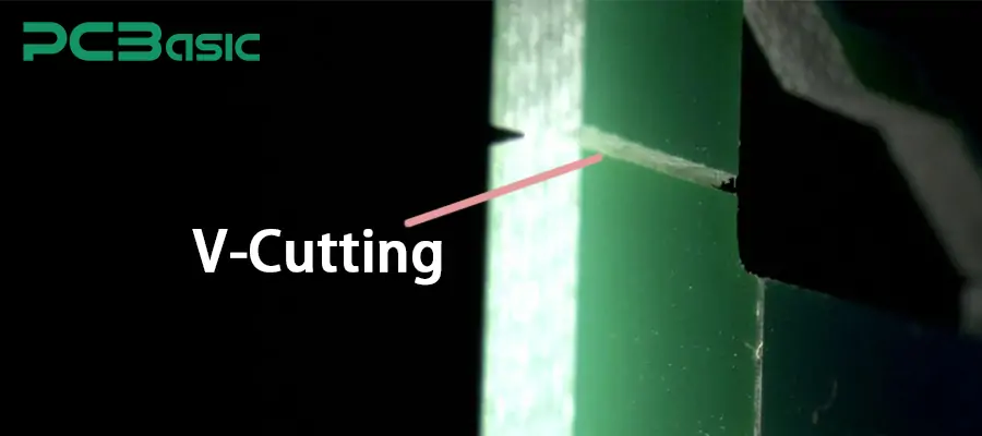
V-scoring is cutting a V-shaped groove into the panel from both sides on the laminate of the printed circuit board to make it easier to remove the individual parts from the V-score PCBs. The V-score PCBs require different scoring tools, including a top & bottom cutting blade run across the panel in a straight line.
Panelized circuit board panels are not feasible to use a V-groove method; opt for the tab routing method. In this method, the panelized PCBs are pre-cut from the array and then held in place on the board with perforated tabs. There are 3-5 holes used in the perforation patterns.
Breakaway tabs are weak points along the edge of the PCB. After the manufacturing process is complete, these tabs can be easily broken or removed. There are different benefits, such as easier handling and easy separation of multiple boards from a single panel.
A mouse bite in a circuit board panel is typically small, semi-circular cutouts or perforations along the edges of the PCB panel. The cutouts resemble small nibbles, which is why they are called mouse bites.
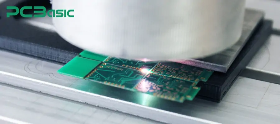
Laser cutting is a PCB depanelizing method, which is the most modern and promising process for PCB separation. As the name suggests, a laser beam is used to cut the individual PCB boards from the large PCB panel.
PCB panelization is a crucial process in modern electronics manufacturing, offering many benefits, such as improved efficiency, better quality control, and reduced electronic waste. Grouping multiple small PCBs into a single panel allows businesses to optimize their production and material use and maintain product integrity.
However, the design and layout are critical, as many considerations, such as size, edge clearance, and separation methods, play a crucial role in a final product's success. There are different types of PCB combinations, such as uniform, mixed, and matrix designs, that allow manufacturers to meet diverse production needs.
Depanelization, or separating individual PCBs from the panel, is important. Different methods, such as V-scoring, tab routing, and laser cutting, provide flexible/precise ways to depanelize boards with menial damage and efficient production. Therefore, by following the proper guidelines, manufacturers can achieve cost-effective, high-quality, and scalable electronic production with PCB panelization, making it a necessity for successful modern electronics manufacturing.
 About PCBasic
Time is money in your projects – and PCBasic gets it. PCBasic is a PCB assembly company that delivers fast, flawless results every time. Our comprehensive PCB assembly services include expert engineering support at every step, ensuring top quality in every board. As a leading PCB assembly manufacturer, we provide a one-stop solution that streamlines your supply chain. Partner with our advanced PCB prototype factory for quick turnarounds and superior results you can trust.

Assembly Enquiry
Instant Quote
Phone contact

+86-755-27218592
In addition, we've prepared a Help Center. We recommend checking it before reaching out, as your question and its answer may already be clearly explained there.
Wechat Support

In addition, we've prepared a Help Center. We recommend checking it before reaching out, as your question and its answer may already be clearly explained there.
WhatsApp Support

In addition, we've prepared a Help Center. We recommend checking it before reaching out, as your question and its answer may already be clearly explained there.