Multilayer printed circuit boards (PCBs) have become ubiquitous in the modern electronics industry. Their compact design and ability to efficiently route signals and power allow more complex circuitry to be packed into increasingly small form factors. Analysis shows that the global multilayer PCB market may grow from USD 82.36 Billion in 2022 to USD 128.5 Billion by 2030, at a CAGR of 5.68%.
This enables the development of advanced technologies across various applications – from consumer devices to industrial machinery. However, the intricate multilayer fabrication also poses substantial design and manufacturing challenges.
This article provides a comprehensive overview of multilayer PCB technology. It explores the manufacturing steps involved, layer stack-up considerations, and signal routing. You'll also get to learn about the advantages and limitations along with standard applications.
What is a Multilayer PCB


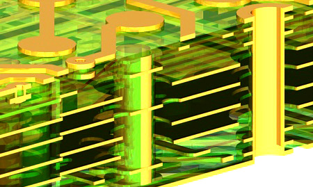
A multilayer PCB is a circuit board that contains three or more conductive layers of copper or other metal, separated by insulating material known as prepreg or core material. While traditional PCBs are usually double-sided with copper traces on the top and bottom, multilayer PCBs stack multiple inner layers of circuitry between the external layers.
There can be many layers, ranging from 4-12 layers commonly. Some devices, like smartphones, can use up to 40 layers. The active and passive components are placed on the outer top and bottom layers, while the inner stacked layers are used for routing traces between components.
This complex multilayer structure allows much higher density circuitry and interconnectivity than conventional single-sided or double-sided boards.
With additional internal layers, multilayer PCBs can accommodate many more electrical components and allow intricate routing of pathways between them. The layers are interconnected using plated through holes or vias, vertical connections between the stacked layers. Different styles like through-hole, buried, or blind vias give designers options to optimize circuit routing.
The multilayer construction makes PCBs well-suited for demanding applications like telecommunications hardware, complex embedded systems, and other situations where miniaturization and high-speed signaling are priorities. Of course, the additional design and manufacturing complexity also makes multilayer boards more expensive than conventional single-layer or double-sided PCBs.
How are Multilayer PCBs Made
Multilayer PCBs provide a higher density of circuitry compared to single and double-sided boards by utilizing multiple inner conductive layers that are laminated together with non-conductive material. This complex construction requires a more involved fabrication process than simpler board types.
The process begins with carefully stacking the raw material layers according to a predetermined sequence and proceeds through several interdependent manufacturing stages to build the finished circuitry on all layers.
Here is an in-depth outlook on the key steps in producing a multilayer PCB.

Stackup Assembly
The first step in the fabrication of a multilayer PCB is stack-up assembly. Different thin layers of prepreg and copper foil sheets are precisely stacked together according to the predetermined layer stack-up order.
The stacks usually contain an odd number of dielectric layers interleaved with inner copper foil and sometimes solid copper layers for power and ground planes.
Lamination
The stacked layers are then sent through a lamination process. During lamination, the stack is placed in a press and exposed to high heat and pressure. This causes the prepreg layers to melt and bond the copper foils and dielectric layers together.
It also drives out any air bubbles trapped between the layers, resulting in a solid laminated sheet. Proper lamination is critical to achieve optimal dielectric bonding and avoid delamination issues in the future.
Panelization
Once the stacking and lamination are completed, the solid sheet is panelized to create individual PCB panel sections. A numerically controlled machine runs through the sheet and cuts it into separate panel pieces according to the predefined panelization file.
Via Formation
Vias are small holes that connect different layers of a multilayer board.
There are three main types of vias used:
● Through-Hole Vias: Passes through all layers of the board.
● Blind Vias: Connects an outer layer to an inner layer but not all through.
● Buried Vias: Connect only to inner layers, which are not visible from the surface.
Through-hole plated vias are typically formed by laser drilling holes at the designated locations before plating the via walls with copper. For buried and blind vias, drilling is done after inner layer patterning.
Inner Layer Patterning
Using a photosensitive film or photoresist, each inner layer panel is selectively exposed to light through a photomask of the desired layer pattern. The exposed material is then developed away or made soluble and washed off. This reveals the copper traces in the intended pattern for that layer.
Plating and Etching
The panel is then electroplated with a thin copper layer to bridge any small gaps in the exposed copper traces. Next, all uncovered copper is etched away using chemicals, leaving behind the plated photoresist pattern as a conductive layer for that inner panel. The photoresist is then stripped away at the end.
Outer Layer Processing
Once all inner layers are complete, outer layer circuits are formed by a similar process of photoresist patterning, plating, and etching. Through-hole vias are also plated to connect to the inner layers at this stage if needed.
Final Operations
The last stages involve finishing operations like solder mask and silkscreen printing, component mounting, and electrical testing before the finished multilayer PCB panels are shipped out.
What Factors Should Be Considered During Multilayer PCB Design and Manufacturing
Designing and manufacturing a multilayer PCB requires considering several important factors to ensure the end product meets specifications. Multiple elements must work seamlessly together from the design phase through production.
Here are some factors to consider.
Number of Layers
One of the first decisions is determining how many internal layers are needed in a multilayer PCB design. More layers allow for increased functionality but also drive up costs and complexity. The stack-up configuration should balance these factors.
Dielectric Material
The dielectric plays a key role in signal integrity and impedance control. Materials like FR-4, polyimide, and Rogers provide different electrical properties that influence stack-up design. Characteristics like dielectric constant must match the intended application.
Trace Width and Spacing
Minimal trace widths and spacing maximize routing while avoiding difficulty in manufacturability or reliability issues. The selected fabrication process tightly governs design rules.
Via Design
Vias connect layers, and their shape, size, and locations desperately impact manufacturability. Plated through-hole, buried, and micro vias each affect stack up and density. Their impact on impedance must also be considered.
Automation and DRC Tooling
The PCB layout, fabrication process, and design rules should be compatible with automation to maximize manufacturability. Effective DRC tooling is critical to catch and correct issues early.
Finishing and Assembly
Factors like outer layer finishes, holes, and manufacturing tolerances determine future processing steps such as assembly, enclosure integration, and environmental sealing.
Advantages of Multilayer PCBs
Multilayer PCBs provide several advantages over traditional single and double-layer boards. By utilizing multiple inner layers, circuitry can be stacked vertically, which results in tremendous space savings.
Some of the key benefits of multilayer circuit boards include:
● Reduced PCB Size. Using multiple inner layers allows components and traces to utilize vertical space instead of just horizontal space. This significantly reduces the overall footprint of the board.
● Lightweight. With multilayer construction, boards can be made thinner while retaining complex circuitry. This makes them much lighter than the equivalent functionality of single/double-layer boards.
● High Quality and Density. Placing components and traces on inner layers increases the routing density and quality of connections between components compared to conventional layered boards.
● Better Durability and Flexibility. The compact multilayer design makes boards more durable since components are protected between layers. They are also more flexible in their applications.
● Powerful with Single Connection Point. Traces can be routed throughout the layers, allowing all I/O to terminate or pass through on a single surface. This simplifies connections.
Disadvantages of Multilayer PCBs
Multilayer PCBs provide many benefits, such as increased circuit density and shortened signal paths. However, their complexity also presents disadvantages compared to simpler single- or double-layer boards.
● Higher Manufacturing and Production Cost: The additional circuit layers and registration processes involved in multilayer boards drive up material and labor costs.
● Complicated Design and Production: With internal signal layers, power planes, and blind/buried vias, multilayer boards require much more sophisticated CAD tools and production techniques.
● Limited Manufacturers: Only board shops with extensive multilayer fabrication capabilities can produce complex multilayer designs. This concentrates production in fewer facilities.
● Highly Skilled and Trained Designers Are Required: Effective design of internal layers and routing within a multilayer stack demands experienced PCB engineers familiar with 3D circuit design.
● Increased Production Time: The extra steps of layer registration, inner layer fabrication, lamination, and drilling inevitably lengthen the time needed to manufacture a multilayer board compared to a simpler multilayer board.
Multilayer PCB Applications
Multilayer printed circuit boards (PCBs) are widely used in electronics due to their high-density packaging capabilities. Look at some key applications of multilayer PCB technology across different industries.
Computers
Multilayer PCBs allow complex circuit designs with numerous components to be fitted on a compact motherboard. They facilitate faster data transfer between the CPU, memory, graphics card, and other peripherals. High-layer count PCBs with buried vias efficiently route power and signal traces within desktops, laptops, and other computing devices.
Cell Phones
Cell phone PCBs utilize tightly packed multilayer designs to accommodate an extensive list of components like processors, memory chips, radio circuits, touchscreen drivers, and cameras. They enable advanced smartphone functions like 4G/5G connectivity, WiFi, Bluetooth, GPS, and NFC. Compact repeater PCBs built with buried vias boost cell signals in areas with weak reception.
Industrial Controls
Multilayer control boards with surface mount technology integrate microprocessors, sensors, actuators, and I/O in programmable logic controllers, CNC machines, industrial robots, and power generators. They reliably manage complex embedded processes in industrial automation.
GPS Systems
GPS receivers employ multilayer PCB layouts to synchronize high-frequency electronic signals from multiple satellite sources precisely. This facilitates rapid triangulation of positional data for navigation applications in aircraft, vessels, and vehicles.
Test & Measurement Equipment
Precision instruments for R&D and manufacturing, like oscilloscopes, spectrum analyzers, and function generators, rely on multilayer circuit board construction to precisely route microwave and RF test signals. This ensures measurement accuracy at high operating frequencies.
Medical Devices
Multilayer PCBs feature in diverse medical appliances like ultrasound and X-ray machines, ECG/EEG monitors, and defibrillators due to their ability to efficiently distribute low-level biological signals. Their reliability and miniaturization enable the portability of lifesaving equipment.
Nuclear Applications
Buried transmission line techniques on multilayer boards allow stable routing of high-power signals in nuclear detection and security systems. They securely transmit sensitive data from radiation sensors to control interfaces.
Aerospace Engineering
Spacecraft satellites employ robust multilayer designs fried under vacuum. Complex routes are achieved through densely packed layers for command/data handling, power control, and instrumentation in satellites, space stations, and probes.
Traffic Management
Intelligent transportation systems leverage multilayer PCB networking to link traffic sensors, cameras, and message signs. They facilitate efficient traffic coordination across smart city infrastructures.
That covers some major applications of multilayer PCB technology across computers, consumer electronics, industrial automation, test & measurement, medical appliances, defense, aerospace, and transportation systems. Its capabilities for miniaturization and tight component packaging have made it indispensable in modern electronics.
FAQs About Multilayer PCBs
1). Why Are Multilayer PCBs Commonly Used?
Multilayer PCBs are commonly used because they allow for much higher component density and functionality than traditional single and double-sided ones. By adding internal layers, multilayer PCBs enable vertical routing of circuit traces, which saves a significant amount of board space, making them ideal for applications that require miniaturization, like consumer electronics, telecom equipment, and various control systems.
The high density achievable with multilayer PCBs also means reduced product sizes, improved performance through shorter signal paths, and improved power distribution.
2). How Much Does a Multilayer PCB Cost?
The cost of a multilayer PCB depends on several factors: the number of layers, the board size, the complexity of circuit design, material choices, etc. In general, multilayer circuit boards are more expensive than single or double-sided boards due to the increased complexities of design and manufacturing.
A basic 4-6 layer board may cost between $150 to $300 per square foot, depending on quantities. High-density boards with 8-16 layers often range from $300 to $800 per square foot. Complex boards with over 16 layers cost over $1000 per square foot. Overall, the per-layer cost increment tends to decrease with increasing layer counts as manufacturing efficiencies improve.
3). Can a PCB Have 3 Layers?
Yes, a PCB can have three layers. Three-layer boards are quite common and represent the basic multilayer PCB configuration after double-sided boards. The three layers enable horizontal placement of components on the top and bottom layers, with circuit traces routed internally in between.
This level of vertical integration allows for addressing complexity issues faced by double-sided boards. Three-layer boards strike a nice balance between capabilities and costs, making them suitable for many applications that need basic multilayer functionality without high-density requirements.
4). What Materials Are Used in Multilayer PCBs?
The most common materials used in multilayer circuit board fabrication include FR-4 fiberglass epoxy laminate, polyimide laminates, and various specialized high-frequency and high-temperature materials.
FR-4 is the most widely used laminate due to its superior balance of electrical properties, mechanical strength, and affordability. Polyimide materials offer higher thermal resistance, dimensional stability, and Mil-Spec compliance, which is useful for defense and aerospace applications.
Ceramic-filled PTFE laminates provide extremely high withstand voltages needed in power electronics. Multilayer boards also employ prepreg dielectric materials, often composed of woven fiberglass cloth embedded with partially cured epoxy resin, to bond individual layers during lamination. Precious metal plated through holes and traces using copper, gold, or other metals enables electrical connections between stacked layers.
5). What Are the Features of Multilayer PCB?
Key features of multilayer PCBs include:
● Increased layer counts (4-16+ layers common) for highly complex 3D circuit designs;
● Vertical routing to minimize board space and trace lengths;
● Very high component density and integration capabilities;
● Improved electrical performance due to shortened traces;
● Simultaneous mounting of components on multiple surfaces;
● Robust power/ground planes for low impedance and EMI prevention;
● Compatibility with a mix of surface mount and through-hole components;
● Increased usable surface area on inner layers;
● Uniformity and repeatability from automated lamination processes;
● Wide range of applications spanning electronics, medical, automotive, etc.
Conclusion
Multilayer PCBs have become a vital part of our increasingly technological world. Multilayer boards have enabled innovations like smartphones, advanced medical devices, autonomous vehicles, and more by allowing tighter packing of circuit elements and the creation of more complex circuit designs.
As electronics continue to shrink in scale while growing in capabilities, multilayer PCBs will remain an important technology for fitting ever-greater functionalities into smaller spaces. While designing and manufacturing multilayer boards presents challenges, the ability to build stacked circuitry creates new possibilities.
As long as the demand exists for more advanced electronics, multilayer PCBs will continue to play a central role in achieving greater integration and performance. They have indeed become the foundation for innovation across many industries.