
Global high-mix volume high-speed PCBA manufacturer
9:00 -18:00, Mon. - Fri. (GMT+8)
9:00 -12:00, Sat. (GMT+8)
(Except Chinese public holidays)





HomePage > Blog > Knowledge Base > Smart Meter PCB Assembly: From Accurate Metering to Reliable Production
1. What Is Inside a Smart Meter PCB?
2. What Makes Smart Meter PCB Assembly Different?
3. How Smart Meter PCB Assembly Moves Through Production
4. How Is a Smart Meter PCBA Tested?
This also means that a smart meter PCB cannot merely be able to "function when powered on". It also has to ensure that measurements are accurate, communications are reliable, and results are consistent. The performance of the final product in case of smart meter PCB assembly depends on current sensing, key components, communication modules, soldering and testing.
This article will introduce the main components, assembly process, and key smart meter testing that need to be focused on before mass production from a manufacturing perspective for smart meter PCBA.
A smart meter PCB is more than just one board that holds all of the components together. The functions of metering, data processing, power management, communication and control need to work in coordination. The designs of different products may vary, but most smart meters will include some similar basic modules.
Inside a typical smart meter PCB, you will usually find:
• Metering IC or analog front-end
• MCU
• Voltage and current sensing circuits
• Power supply
• Memory and real-time clock
• Communication module
• Display interface
• Tamper-proof detection circuit
• Relay or load control components
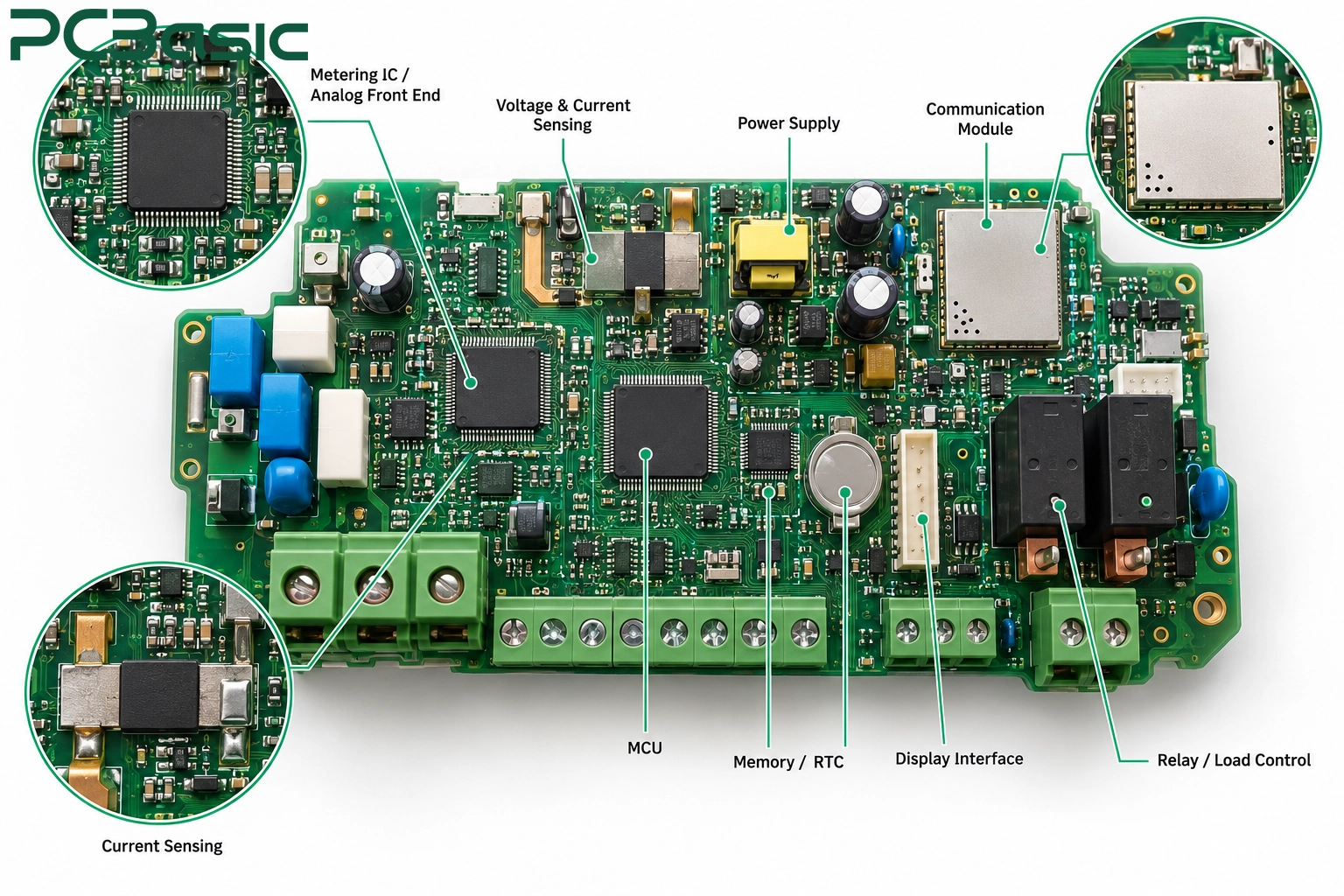
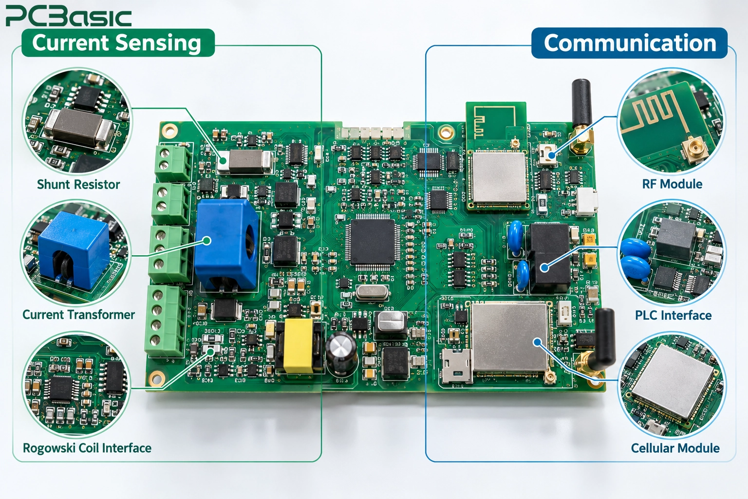
So how does a smart electricity meter actually measure electricity use? The key lies in the metering part. It needs to first collect voltage and current signals. Depending on the design, the current can be detected through shunt resistors, current transformers, or Rogowski coils.
The metering IC or analog front-end will then transform these signals into digital data, which will be passed to the MCU for further processing. The MCU is responsible for more than just simple calculations; it can also calculate energy, store data, manage the display, and execute time-based invoicing activities.
An energy meter PCB requires high accuracy. Temperature changes, resistor tolerance, and sampling precision can all have an effect on the measurement results. Therefore, these key components cannot be replaced randomly.
A smart meter PCBA also needs stable power supply and the transmission of data. For example, AMI smart meter can exchange data with the back-end system in the advanced metering infrastructure through PLC, RF, cellular communication, or other methods.
In addition, the board may also have backup storage, real-time clock, tamper-proof detection, display control, and load disconnection functions. Some designs may also use larger relays, which are often not directly part of the complete SMT process but require subsequent separate assembly.
When these modules are combined, they form a truly smart meter PCB that can complete measurement, processing, storage and communication.
Many common manufacturing stages are used in smart meter PCB assembly, including solder paste printing, component placement, reflow soldering, through-hole PCB assembly, inspection, and testing. The difference is that small changes in the sensing circuitry, component values, PCB design, or the quality of assembly can directly impact the metering accuracy and communication performance.
A smart electricity meter's PCB must manage accurate measurements, circuits for mains power, digital processing, and communication features all at the same time. Therefore, when producing such boards, we cannot only focus on the soldering quality. Key components, isolation, thermal characteristics, calibration, and testing also need to be controlled well.
|
Method |
Main Advantage |
Primary Manufacturing Considerations |
|
Shunt resistor |
Compact size, lower cost |
Resistance tolerance, heat, and sense-trace routing |
|
Current transformer |
Provides electrical isolation |
Size, placement, and phase characteristics |
|
Rogowski coil |
Supports a wide current range |
Requires additional signal-conditioning circuits |
The current sensing method used will have a direct impact on how we layout the PCB, isolate components, arrange them, calibrate, and test the smart meter. As a result, if we need to change important sensing components throughout the manufacturing process, we must first determine whether the original metering and calibration results will be impacted.
|
Method |
Main Features |
PCB / Assembly Considerations |
|
PLC |
Transmits data over existing power lines |
Coupling, filtering, and protection circuits |
|
RF |
Wireless communication |
Antenna placement, RF layout, and noise control |
|
Cellular |
Wide-area connection |
Modem, antenna connection, and peak power consumption |
In real projects, we choose the right way to communicate with AMI smart meters depending on the situation they're used in, the network they're connected to, and what the product needs. For example, the RF-based smart meter IoT design will focus more on how to arrange the antenna and manage signal interference, while PLC and cellular communication methods will have different needs when it comes to power usage and protection.
So, even if the metering circuits of two smart energy meter look similar, we may adopt completely different methods in PCB layout and production control. This is exactly where the difference is between smart meter PCB assembly and standard SMT assembly.
Reliable smart meter PCB assembly actually begins even before the machine production. Are the materials correct? Are there any issues with the packaging and polarity? Can the key sensing components be replaced? Are the isolation distances and test points in compliance with the requirements? All of these need to be confirmed first.
For energy meter PCB, this step is particularly important. Because if the precision resistors, sensing device or power components change, the subsequent calibration results and metering performance may be affected.
Once the materials are verified, the SMT process can begin. First, solder paste is applied, and then an SPI inspection is done to check that the area, position, and amount of solder paste are correct, helping to avoid issues before the mounting process begins.
Next, the pick-and-place machine will install the MCU, metering IC, passive components, communication devices, and other SMD components. Once the reflow soldering process is done, an AOI inspection is carried out to identify typical problems like:
• Missing or incorrect components
• Polarity error
• Component placement offset
• Solder bridge
• Visible solder joint defects
What if the solder joints are underneath the component and can't be seen by the automated optical inspection system? In such cases, X-Ray inspection can be added.
In PCBasic, the smart meter PCB assembly project can be completed by combining SMT, SPI, AOI, X-Ray, BOM management and production traceability. For smaller SMD or fine-pitch components, we will also set up suitable assembly and checking methods based on the specific design.

Smart meter PCBA may not be all SMT components. Relays, terminals, transformers, connectors, and various current-sensing devices frequently use through-hole designs due to their size, mechanical strength, or current-carrying needs.
How should these parts be assembled? It depends on the design. DIP, wave soldering, and selective wave soldering can be used. Controlled manual soldering is also an option in some instances. Especially when there are both precision small components and large current-carrying components on a single board, how the previous and subsequent processes are connected is very important.
Before formal production, we also need to confirm whether the substitute materials have been approved, whether the assembly method is compatible, whether the inspection standards are clear, and whether the test points are available. Cost is of course a consideration, but it should not affect the metering accuracy, safety, or certification requirements due to cost pressure.
Through these processes, PCBasic can assist in transitioning the smart meter PCBA from prototype manufacturing to stable and repeatable large-scale production.
After the smart meter PCBA is completed, its appearance seems fine, which only tells us that the assembly is basically successful. Can it meter accurately, communicate stably, and is there any functional problems? We still need to conduct further tests.
Therefore, the smart meter testing usually does not involve only one test. Different tests focus on different issues, and the absence of any one layer may leave a blind spot.
Let's look at the soldering and component placement. Before reflow soldering, SPI can check the solder paste printing situation; after reflow, AOI will then check for missing parts, reverse, offset, solder bridges, or visible solder-joint defects.
Some solder joints are hidden beneath the components and cannot be seen by AOI. In such cases, X-Ray inspection is needed.
After the appearance and soldering are fine, we need to confirm the electrical connections. Flying probes or ICT can check for open, short circuits, connection status, and some key test points.
In PCBasic, we do not apply the same testing process to all projects. The board structure, the number of test points, and the production volume all differ, and the combination of test methods used will also vary.
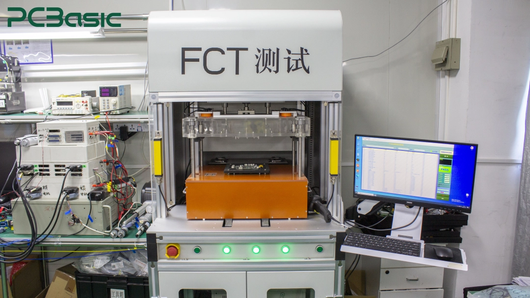
The fact that the circuit is connected does not mean that the board is truly "usable".
During the function testing, we will have the smart meter PCB run on the fixture to check communication, display, relays, I/O, and other specified functions.
But for the meter, there is one thing that is more crucial: is the measurement accurate?
A complete electricity meter or smart energy meter also needs to be calibrated and verified for accuracy according to product requirements, accuracy grades, and target markets. In other words, even if ICT or FCT passes, it only indicates that the electrical and functional performance of the board is basically normal. But it does not mean that the overall metering accuracy of the entire meter has been confirmed.
During the prototype stage, it is sufficient to confirm that a board can operate. In mass production, the focus changes: this batch can pass, but can the next batch maintain the same?
At this time, BOM changes, test procedures, calibration parameters, inspection standards, and traceability records need to stay under control.
For the AMI smart meter and smart meter IoT project, we can also associate the board number, batch, and corresponding test data. PCBasic helps the smart meter PCBA from prototype verification to gradually enter stable mass production through IQC, first-article inspection, MES traceability, and PCBA functional testing.

For a smart meter PCB assembly project, the real challenge is not to make a board work properly, but to ensure that the same design can be consistently produced, tested clearly, and yield consistent results across different batches.
A well-prepared production process helps reduce variations, avoid unnecessary rework, and makes it easier to expand production scale later. For manufacturers and product teams, it is this consistency that turns a working prototype into a product suitable for mass production.
If you are preparing for the production of a smart meter PCB prototype or volume production, PCBasic can provide DFM review, component sourcing, PCB assembly, testing, and traceable production support. Contact PCBasic to discuss your project requirements and get a quote.
Q1: What components are typically found on a smart meter PCB?
Typical smart meter components include a metering IC, MCU, current- and voltage-sensing circuits, power supply, memory, display interface, communication circuitry, and sometimes relays or tamper-detection devices.
Q2: What is the difference between a smart meter PCB and a smart meter PCBA?
A smart meter PCB is the bare printed circuit board. A smart meter PCBA is the assembled board after electronic components have been mounted and soldered.
Q3: How is a smart meter PCBA tested?
Smart meter testing may include SPI, AOI, X-ray where needed, flying probe or ICT, functional testing, communication checks, and product-level calibration or accuracy verification.
Q4: Do smart meter PCBs use SMT or through-hole assembly?
Most smart meter PCB assembly uses SMT for ICs and small passive components, while relays, terminal blocks, connectors, and other larger parts may require through-hole assembly.
Assembly Enquiry
Instant Quote


Phone contact

+86-755-27218592
In addition, we've prepared a Help Center. We recommend checking it before reaching out, as your question and its answer may already be clearly explained there.
Wechat Support

In addition, we've prepared a Help Center. We recommend checking it before reaching out, as your question and its answer may already be clearly explained there.
WhatsApp Support

In addition, we've prepared a Help Center. We recommend checking it before reaching out, as your question and its answer may already be clearly explained there.
