Global high-mix volume high-speed PCBA manufacturer
9:00 -18:00, Mon. - Fri. (GMT+8)
9:00 -12:00, Sat. (GMT+8)
(Except Chinese public holidays)


Global high-mix volume high-speed PCBA manufacturer
9:00 -18:00, Mon. - Fri. (GMT+8)
9:00 -12:00, Sat. (GMT+8)
(Except Chinese public holidays)


HomePage > Blog > Knowledge Base > Understanding Camera PCBs
Cameras find a place under innovation in the modern world of electronics, combining advanced functionality in a compact design. Camera PCBs are specialized types of printed circuit boards that will form the backbone for industrial cameras, from security applications to medical imaging devices, depending on the requirement. Understandably, as the performance of cameras is increasingly and constantly in demand, being aware of the role and importance of Camera PCBs will help.
Market analysis recently shows that the camera module market will grow to over $60 billion by 2028, with mini cameras gaining wide acceptance in smartphone and wearable devices, as well as in industrial applications. Behind those sharp images and smooth video recordings are cameras, the unsung heroes in today's high-tech lives because they can combine multiple components into one single board.
It covers the major constituents, functions, and applications of camera PCBs while incorporating other elements that make them indispensable in today's high-tech world.
A PCB camera is one really complex but very well-designed system in which each component plays its role for optimal functionality. So, let's break down the crucial elements.
Light is converted into electrical signals by the image sensor, which is the heart of a camera. The two main industry players are CMOS and CCD (Complementary Metal-Oxide Semiconductor and Charge-Coupled Device). The best sensor for given applications varies, but good-quality sensors image excellent color reproduction and low-light performance, which are fundamental for security and inspection devices.
In fact, the lens' ability to focus incoming light onto an image sensor will essentially determine the sharpness of any image captured. However, high-grade lenses can also feature either optical zoom or wide-angle capability, making a camera much more adaptable in different environments, from smartphones to surveillance systems.
It captures raw data from the sensor and enhances the image by eliminating distortion, increasing clarity, and color balancing. Obviously, it plays an integral part in preventing bad photos and videos in all fields, most significantly the highly demanding areas of health and space research.
The most important part that saves the captured images and videos is memory. It might also be volatile memory for only just-in-time processing or nonvolatile memory for longer-term retrieval.
Connectors connect the camera PCB to numerous displays, processors, and storage devices. As such, they must be reliable and efficient enough to achieve full communication without loss of data.
A good camera PCB is power-efficient because of the power management circuit that manages and distributes the power to all constituents. This must be for a stable device that can be used longer in power-sensitive applications like wearables.
The base itself works as a printed circuit board where all the components are combined by supporting them. Advanced PCB design allows proper utilization of space to allow even mini cameras of exceptional quality without compromising on size.
Apart from the basic ingredients of Camera PCB, most of them contain other elements such as infrared filters for better night vision, a built-in microphone, or LEDs for extra light. All these ancillary components add additional capabilities to Camera PCB for particular applications.
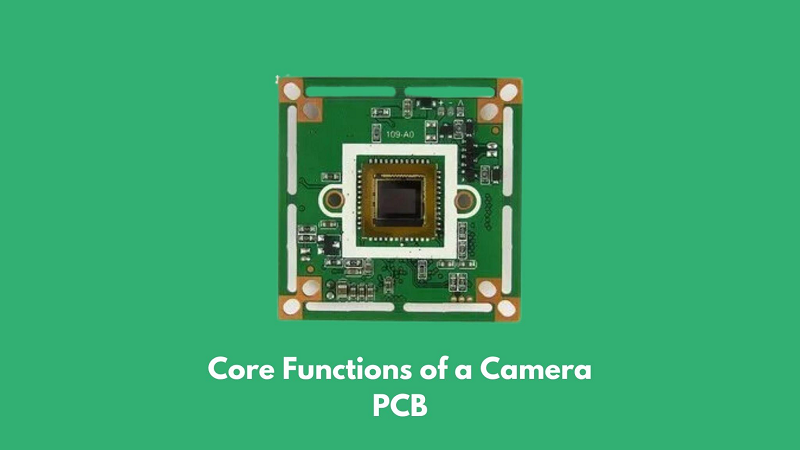
More than the simple collection of components, the camera PCB is a dynamic system that allows several functions that are considered critical in modern imaging. These are the basic and advanced functions that it performs:
The core competency of a PCB camera lies in capturing ability and such an optical signal conversion into a digital one. In the given context, an image sensor is considered the cornerstone element because it calculates and computes the intensity levels with the color to display an initial raw image for further operations.
The raw data needs to be processed by this sensor. The image processing unit corrects distortion, enhances clarity, and adjusts color balances. Advanced signal processing is applied to ensure the output meets the specific needs it is used for in areas such as security or medical imaging.
Any camera PCB board must consume power efficiently. Power management circuitry ensures the distribution of electricity to every component without overloading them, which stabilizes operations and lengthens the lives of the batteries in portable devices such as mini cameras and inspection tools.
An A Camera PCB transfers processed image or video data to other devices such as displays, storage systems, and external processors. High-speed connectors and interfaces ensure consistent communication with high-resolution data.
The camera on the PCB allows control of most components it comprises to run in conjunction. Coordination ensures the running of all operations like Autofocusing, setting of correct exposure and the high speed without any delay.
The Camera PCB uses image compression methods for the optimal storage and transmission of images. This feature reduces the file size of photos or videos without quality loss, thus relieving the constraint on storage or bandwidth.
Knowing the technical parameters of a PCB board for any camera will assist in the right design for any application. Here are the most important specifications:
Resolution determines the amount of detail an image can capture. High-resolution Camera PCBs are very important in industries like healthcare and surveillance, where precision is of utmost importance. Now, a resolution of 4K or higher is quite common in advanced systems.
The sensitivity of an image sensor determines how a camera would do well in low light. Images from highly sensitive sensors are, in general, measured in fluxes, which allows security cameras to capture clear images during the night.
The frame rate, measured in frames per second (fps), defines the smoothness of video capture. For the application to sports videography or high-speed inspection devices, it should use a higher frame rate.
This shutter speed controls the amount of light that hits the sensor. Higher shutter speeds capture movement much more clearly, and slower shutter speeds enhance the low-light performance. Thus, the goal is the balance that will provide sharper, better-lit images.
High-quality lenses ensure the proper focusing of light onto the sensor. Distortion to this is minimum, while clarity to this is maximum. Lens coatings and optical zoom affect performance overall.
Modern cameras contain high-end technologies inside their PCBs, including AI-based object recognition and HDR imaging with thermal sensors, that enhance functionality to fit the niche usage for various specialized applications in either the automotive or aerospace sectors.
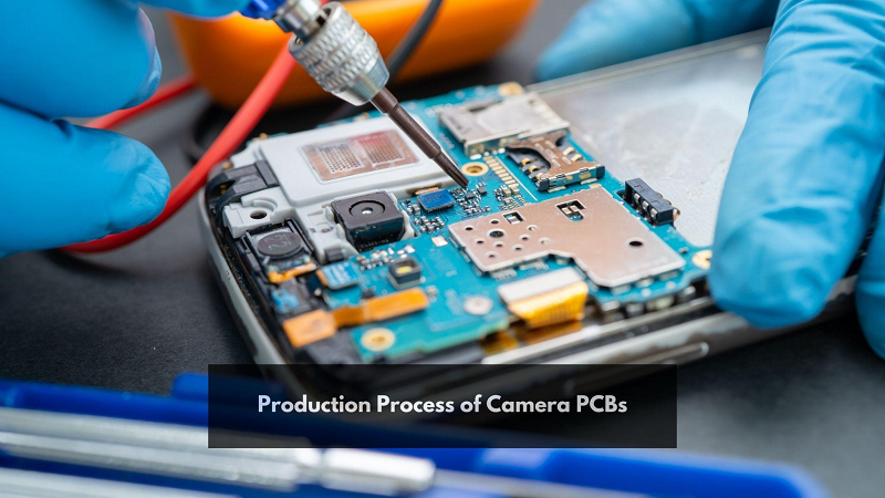
Producing a Camera PCB involves several meticulously executed stages, each crucial for ensuring quality and reliability.
Mass production starts only after thorough design, during which engineers use advanced software, such as Altium Designer or Eagle, to come up with really detailed schematics. Afterward comes prototyping, whereby initial designs are tested before mass production is initiated.
A PCB is printed in the fabrication. The high-grade FR4-a fiberglass-reinforced laminate is used to give shape to multi-layered PCBs in this process. Techniques that involve lamination and etching have more precision and hardness in PCBs.
The assembly process involves mounting components such as sensors, lenses, and processors onto the PCB. Automated assembly techniques like surface-mount technology enhance the accuracy and efficiency of assembly.
Testing is very critical to the reliability of the camera PCB board. It passes through many rigorous quality control tests, including functionality tests, environmental stress tests, and visual checks for defects and rectification. Only after passing all these tests can a PCB be put into service.
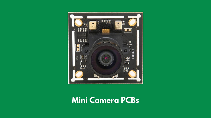
Many modern imaging systems feature camera PCBs, which can be used in all walks of life. Here's how different sectors find these compact-sized, power-enabled mini-camera PCBs:
Mobile photography became ever more revolutionized when even very small high-performance mini-camera PCBs may bring up multiple sensors' optical zoom capabilities and AI-driven features.
From CCTV systems to smart home devices, camera PCB plays a very important role in surveillance. They assure high-resolution imaging, night vision capabilities, and real-time video streaming, making them irreplaceable in security systems.
Most industrial precision manufacturing processes and some maintenance work require these mini-camera PCBs because they enhance the means of detecting damage and defects through machinery, electronic devices, or pipeline breakdown.
Camera PCBs are very crucial in capturing images and videos in space, especially in extreme conditions. The required strength and robustness needed for such high radiation levels, extreme temperatures, and microgravity will be in a PCB, which could function very well.
ADAS and autonomous cars depend on Camera PCBs for functionality and service operation. ADAS enhances security and ease through solutions such as lane detection and parking guidance powered by reliable, efficient imaging solutions.
When product contents include a camera PCB, the companies require OEM as well as ODM. Let me simplify those acronyms and their worth:
● OEM: Solutions here include designing Camera PCBs to a particular requirement that happens to find its way into company-branded products.
● ODM stands for Original Design Manufacturer. The manufacturers here offer pre-designed PCBs that can be ordered according to requirements.
OEM and ODM solutions target several markets by offering custom designs that address a given need. Examples include:
● Medical Equipment: PCB board of an endoscope or diagnostic imaging.
● Consumer Electronics: Extremely thin PCB for wearable cameras.
● Aerospace: Toughest design for high altitude or space applications.
● Better functionality: Functional designs for a specific purpose.
● It is cost-effective: It is designed with no unscrupulous features.
● Shorter Time-to-Market: Pre-defined options save development time.
● Scalability: Scalability should be easy for several product lines or markets.
With OEM and ODM solutions, it would help the companies enjoy the efficiency of PCBs for cameras and reliability with their market flexibility.
Camera PCBs form the backbone of many inventions, the smartphone in your pocket or the automobile on the road. This paper shall trace its constituents, specifications, and application to highlight the versatility and further the importance of modern technology.
Camera PCBs represent the backbones of every greatness in imaging for security, automobiles, healthcare, and even outer space. OEM and ODM solutions take the lead on this with the amount of exact customization required to give visions life.
Want a custom Camera PCB to change your product? Look at your options today and take your first step toward imaging innovation!

Assembly Enquiry
Instant Quote
