
Global high-mix volume high-speed PCBA manufacturer
9:00 -18:00, Mon. - Fri. (GMT+8)
9:00 -12:00, Sat. (GMT+8)
(Except Chinese public holidays)





HomePage > Blog > Knowledge Base > BGA PCB Assembly: Process, Design Rules, Inspection, and Quality Control
Modern electronic products are becoming smaller, faster, and more complex. From industrial controllers and medical devices to communication modules and consumer electronics, many products now require high-density circuit layouts and reliable signal performance. This is one reason why the ball grid array package has become widely used in PCB design and manufacturing.
Unlike traditional leaded components, BGA packages use solder balls arranged under the component body. This structure saves board space, supports more I/O connections, and improves electrical and thermal performance. However, it also makes BGA PCB Assembly more difficult than standard SMT assembly because the solder joints are hidden under the package and cannot be inspected visually.
For engineers, buyers, and hardware teams, understanding BGA assembly is important before starting a project. This article explains the main process, key design rules, common defects, inspection methods, and how to choose a reliable BGA PCB assembly manufacturer.
BGA PCB Assembly is the process of mounting BGA components onto a printed circuit board using surface mount technology and reflow soldering. BGA stands for Ball Grid Array. Instead of having pins or leads around the edge of the package, a BGA component has many solder balls arranged in a grid pattern on the bottom side.
During assembly, solder paste is printed onto the PCB pads. Then the BGA chip or package is placed on the board by a pick-and-place machine. When the board passes through the reflow oven, the solder paste and solder balls melt and form connections between the package and the PCB.
A typical BGA packaging structure includes the semiconductor die, package substrate, internal bonding or interconnection structure, encapsulation material, and solder balls. The solder balls are placed on the bottom side of the package and act as both electrical and mechanical connection points.
This structure allows BGA chips to support more connections within a smaller area. It is commonly used for processors, memory chips, FPGAs, controllers, and communication ICs.
The solder balls are the key connection points between the component and the BGA PCB. When heated during reflow, the solder balls melt together with the solder paste on the PCB pads. After cooling, they form solid BGA solder joints.
Because these joints are under the component body, they are not visible from the outside. This is why process control and X-ray inspection are especially important in BGA production.
Standard SMT components such as resistors, capacitors, SOPs, and QFPs usually have visible terminations. AOI and visual inspection can check many solder joints directly. In contrast, BGA components have hidden solder joints, so normal visual inspection is not enough.
This makes BGA PCB Assembly more demanding. It requires tighter control of PCB design, solder paste printing, component placement, reflow profile, and post-reflow inspection.
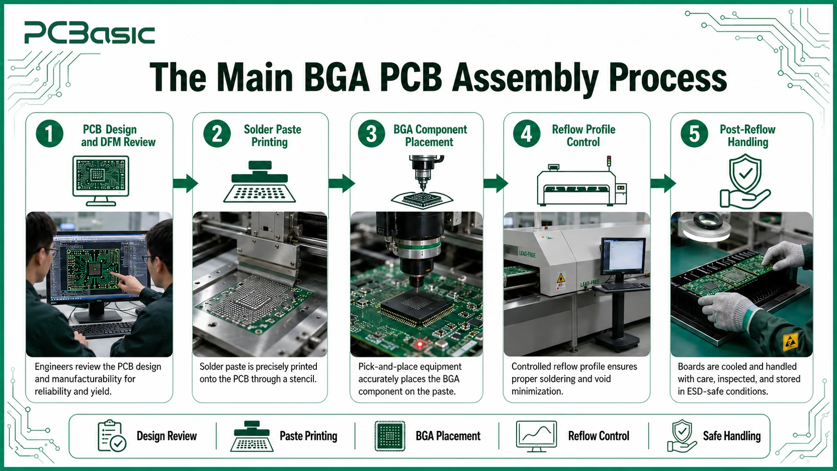
The BGA PCB Assembly process is not only about placing a component on a PCB. It includes design review, material preparation, solder paste printing, placement, reflow, inspection, testing, and sometimes rework verification.
Before production, the manufacturer should review the PCB design files. A good DFM review checks BGA pitch, pad size, solder mask opening, via structure, fanout routing, spacing, stencil design, fiducial marks, and thermal design.
For a complex BGA PCB, this step can prevent many problems before manufacturing begins. If design risks are found early, they are easier and cheaper to correct.
Solder paste printing is one of the most important steps in BGA assembly. The paste volume must be consistent and accurate. Too much solder paste may cause bridging. Too little solder paste may cause open joints or weak solder connections.
Stencil thickness, aperture size, aperture shape, and solder paste condition all affect printing quality. For fine-pitch BGA, solder paste inspection is often recommended to check paste height, area, volume, and offset.
After solder paste printing, the pick-and-place machine places the BGA components onto the PCB. Placement accuracy is very important because even a small offset may affect solder joint formation.
Although BGA packages have some self-alignment during reflow due to solder surface tension, this does not mean placement accuracy can be ignored. Correct orientation, stable placement, and proper machine programming are still necessary.
Reflow soldering is the key step where solder joints are formed. The temperature profile must match the solder paste, PCB material, component requirements, and board thermal mass.
If the temperature is too low, the solder balls may not fully melt. If the temperature is too high, the component may be damaged or package warpage may increase. A proper reflow profile usually includes preheating, soaking, reflow peak, and controlled cooling.
After reflow, the board should be handled carefully. Mechanical stress, sudden temperature change, or improper handling may damage solder joints. For some products, cleaning, conformal coating, or additional inspection may be required.
At this stage, X-ray inspection and electrical testing are often used to confirm the quality of hidden BGA solder joints.

Many BGA problems are not caused only by the assembly line. They may start from the PCB design stage. Good design is the foundation of reliable BGA PCB Assembly.
BGA pitch affects routing difficulty, pad size, solder mask clearance, stencil design, and manufacturing tolerance. Fine-pitch BGA requires tighter design control and more advanced fabrication capability.
The pad design should follow the component datasheet and assembly recommendations. Incorrect pad size may lead to insufficient solder, bridging, or poor joint reliability.
Solder mask defined pads use the solder mask opening to define the pad area. This design can provide better pad anchoring in some cases, but it may also affect solder joint shape.
SMD pads may be used for certain BGA designs, but they should be selected carefully based on the component type, pitch, and reliability requirements.
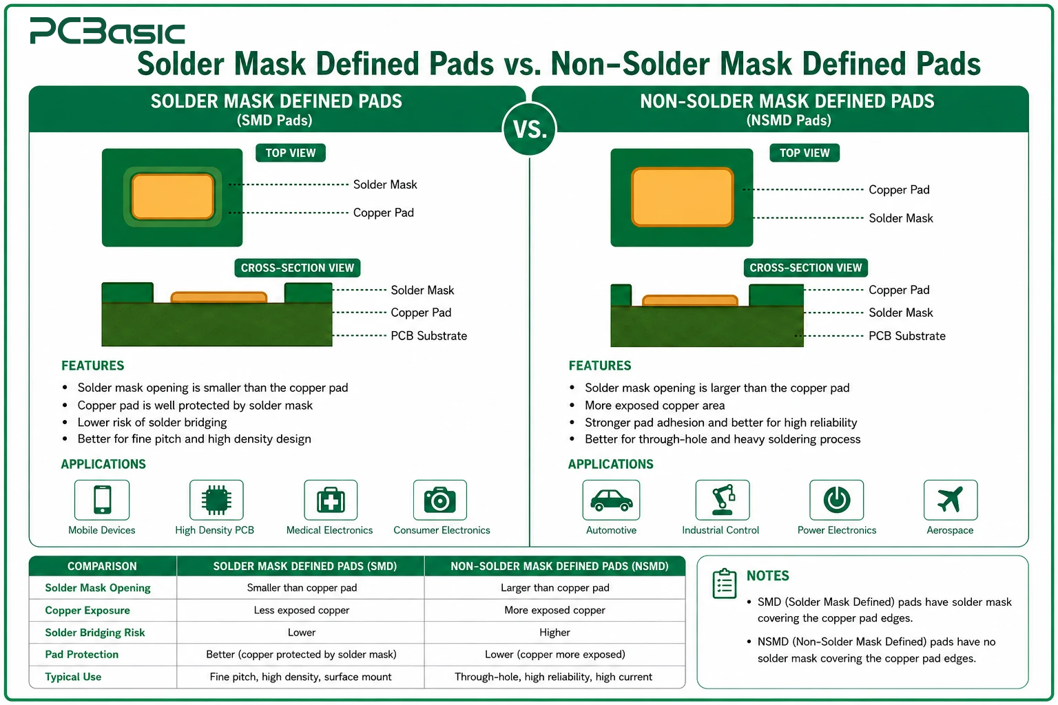
Non-solder mask defined pads, or NSMD pads, are often used in BGA design. In this structure, the copper pad defines the solderable area, and the solder mask opening is larger than the pad.
NSMD pads can help create better solder joint shape and reliability in many applications. However, the final choice should depend on the design requirement and manufacturer capability.
Via-in-pad is often used in fine-pitch BGA or HDI designs. It allows signals to escape from dense BGA areas and helps save PCB space.
However, via-in-pad must be properly filled and planarized. If the via is not filled correctly, solder may flow into the via during reflow, causing insufficient solder volume and open joints.
Dog-bone fanout routing connects a BGA pad to a nearby via through a short trace. This method is common for larger-pitch BGA packages.
For very fine-pitch BGA PCB designs, dog-bone fanout may not provide enough routing space. In that case, via-in-pad or HDI design may be needed.
Stencil design directly affects solder paste volume. For BGA pads, aperture size and shape must be optimized to achieve stable paste release.
Poor stencil design may cause solder bridging, insufficient solder, uneven solder joints, or voiding. For high-reliability products, stencil design should be reviewed together with PCB pad design.
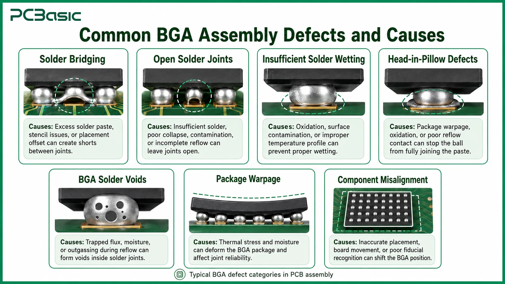
Because BGA solder joints are hidden, defects may not be found by simple visual inspection. Understanding common defect types helps engineers prevent problems during design and production.
Solder bridging happens when two adjacent solder joints are connected by excess solder. It may be caused by too much solder paste, poor stencil design, inaccurate placement, or improper reflow conditions.
For fine-pitch BGA, even a small printing or placement error may cause bridging.
Open solder joints occur when the solder ball does not form a complete connection with the PCB pad. Common causes include insufficient solder paste, poor pad finish, via-in-pad solder loss, contamination, or package warpage.
Open joints can cause complete circuit failure or intermittent electrical problems.
Insufficient wetting means the solder does not properly bond to the pad or solder ball. It may be caused by oxidation, contaminated pads, poor solder paste activity, expired materials, or unsuitable reflow profile.
This defect can reduce solder joint strength and long-term reliability.
Head-in-pillow is a serious BGA defect. It happens when the solder ball and solder paste appear to contact each other but do not fully merge during reflow.
This defect is often related to package warpage, oxidation, poor paste activity, or incorrect thermal profile. It may pass some simple electrical tests but fail later under vibration, temperature cycling, or long-term use.
Voids are empty spaces inside solder joints. Some voiding may be acceptable, but excessive voiding can affect thermal transfer, mechanical strength, and reliability.
Void formation may be related to solder paste, pad design, surface finish, reflow profile, and contamination.
Package warpage happens when the BGA package bends during heating. If the warpage is too large, some solder balls may not contact the pads properly.
This can lead to open joints, head-in-pillow defects, or weak solder connections. Reflow profile control and component storage conditions are important for reducing this risk.
Component misalignment may happen during placement or reflow. Although BGA packages can self-align to some degree, excessive offset may still cause solder defects.
Accurate placement, proper fiducials, and stable PCB support are necessary to control this issue.

Time is money in your projects – and PCBasic gets it. PCBasic is a PCB assembly company that delivers fast, flawless results every time. Our comprehensive PCB assembly services include expert engineering support at every step, ensuring top quality in every board. As a leading PCB assembly manufacturer, we provide a one-stop solution that streamlines your supply chain. Partner with our advanced PCB prototype factory for quick turnarounds and superior results you can trust.
Inspection and testing are critical for BGA PCB Assembly because BGA solder joints are hidden under the package.
The biggest inspection challenge is that BGA joints cannot be seen directly. Visual inspection can only check the component outline, placement condition, and surrounding area. It cannot confirm the internal solder joint quality.
This is why BGA production requires additional inspection methods.
X-ray inspection is one of the most important methods for BGA quality control. It can check hidden solder joints under the package and help detect bridging, opens, voids, misalignment, missing balls, and other defects.
For high-density or high-reliability products, X-ray inspection is not just an optional step. It is a key part of quality assurance.
AOI inspection can still be useful in BGA assembly, but it has limitations. AOI can inspect solder paste printing, component presence, polarity, position, and visible solder joints around other components.
However, AOI cannot fully inspect hidden BGA solder joints. It should be used together with X-ray inspection and electrical testing.
ICT and flying probe testing can check electrical connections and detect some open or short circuits. Flying probe testing is often suitable for prototypes and small batches because it does not require a custom fixture.
ICT is more suitable for stable designs and larger batches. However, electrical testing cannot show the physical shape of solder joints, so it cannot fully replace X-ray inspection.
Functional testing checks whether the assembled board works under real or simulated operating conditions. It can verify power, communication, signal output, firmware operation, and product-level functions.
For complex BGA circuit board products, functional testing helps confirm final product performance.
If a BGA component needs rework, verification is necessary after the rework process. The board should be inspected again by X-ray and tested electrically or functionally.
BGA rework requires controlled heating, accurate alignment, correct solder ball condition, and proper process control. Poor rework may damage the PCB or reduce long-term reliability.

Choosing the right BGA PCB assembly manufacturer should consider from following aspects:
A manufacturer should have real experience with different BGA package types, pitches, board sizes, and product applications. Experience helps the team identify risks early and control defects during production.
For companies sourcing from Asia, many buyers compare China BGA PCB assembly options because China has a strong PCB and PCBA supply chain. However, price should not be the only factor. Capability, communication, inspection, and traceability are more important for long-term reliability.
A good manufacturer should provide DFM feedback before production. They should be able to review BGA pad design, via-in-pad structure, stencil design, spacing, fiducials, and reflow risks.
For new product development, engineering support can reduce trial-and-error and help avoid hidden assembly problems.
Reflow profile control is critical for BGA solder joint quality. The manufacturer should understand thermal profiling, solder paste requirements, package sensitivity, and board thermal balance.
A stable process helps reduce defects such as opens, voids, head-in-pillow, and warpage-related failures.
A reliable manufacturer should have X-ray inspection capability for BGA products. Without X-ray, hidden solder joint quality cannot be properly checked.
When evaluating a China BGA PCB assembly supplier, buyers should ask whether X-ray inspection is available, what defects can be detected, and whether inspection records can be provided.
BGA rework is more complex than replacing standard SMT components. It requires professional rework stations, proper temperature control, accurate alignment, and skilled operators.
A manufacturer with BGA rework capability can better support prototypes, engineering changes, repair needs, and small-batch production.
Traceability helps identify materials, production batches, process records, inspection results, and testing data. For high-reliability products, traceability is very important.
A strong quality system can help reduce risk and provide faster problem analysis if a failure occurs.
PCBasic, a one-stop PCBA manufacturer, supports PCB fabrication, component sourcing, SMT assembly, BGA assembly, inspection, testing, and final delivery. For projects involving BGA PCB Assembly, PCBasic can provide engineering review, process control, X-ray inspection support, and quality traceability with its own MES. Let’s quote for the BGA assembly on PCBasic.com.
BGA PCB Assembly plays an important role in modern electronics manufacturing. BGA packages help save space, support high-density layouts, improve electrical performance, and support better thermal management. At the same time, BGA assembly requires stricter design control, accurate solder paste printing, precise placement, stable reflow soldering, and proper inspection.
Because BGA solder joints are hidden under the package, X-ray inspection, electrical testing, and functional testing are essential for quality control. Many BGA defects can be prevented if the design and process are reviewed carefully before production.
When choosing a BGA PCB assembly manufacturer, buyers should look beyond price. The right partner should have BGA assembly experience, DFM support, reflow process control, X-ray inspection capability, rework capability, and traceability. For companies comparing China BGA PCB assembly services, working with a capable and communicative supplier can help reduce risk and improve product reliability.
BGA PCB Assembly is the process of mounting BGA components onto a PCB using solder paste, placement equipment, and reflow soldering. The solder balls under the BGA package form electrical and mechanical connections with the PCB pads.
BGA assembly is more difficult because the solder joints are hidden under the package. This requires better PCB design, accurate solder paste printing, controlled reflow, X-ray inspection, and reliable testing.
No. BGA solder joints are located under the component body, so they cannot be fully inspected by visual inspection. X-ray inspection is usually required to check hidden solder joint quality.
X-ray inspection can detect hidden defects such as solder bridging, open joints, voids, missing balls, misalignment, and other problems under the BGA package.
Common defects include solder bridging, open solder joints, insufficient solder wetting, head-in-pillow defects, voids, package warpage, and component misalignment.
Common design files include Gerber files, BOM, pick-and-place file, assembly drawing, PCB stack-up information, and special manufacturing or testing requirements.
Choose a manufacturer with BGA assembly experience, DFM support, reflow process control, X-ray inspection capability, BGA rework capability, electrical testing, functional testing, and quality traceability.

Assembly Enquiry
Instant Quote





Phone contact

+86-755-27218592
In addition, we've prepared a Help Center. We recommend checking it before reaching out, as your question and its answer may already be clearly explained there.
Wechat Support

In addition, we've prepared a Help Center. We recommend checking it before reaching out, as your question and its answer may already be clearly explained there.
WhatsApp Support

In addition, we've prepared a Help Center. We recommend checking it before reaching out, as your question and its answer may already be clearly explained there.
