Global high-mix volume high-speed PCBA manufacturer
9:00 -18:00, Mon. - Fri. (GMT+8)
9:00 -12:00, Sat. (GMT+8)
(Except Chinese public holidays)
Global high-mix volume high-speed PCBA manufacturer
9:00 -18:00, Mon. - Fri. (GMT+8)
9:00 -12:00, Sat. (GMT+8)
(Except Chinese public holidays)
HomePage > Blog > Knowledge Base > What is Transparent PCB?| PCB Knowledge
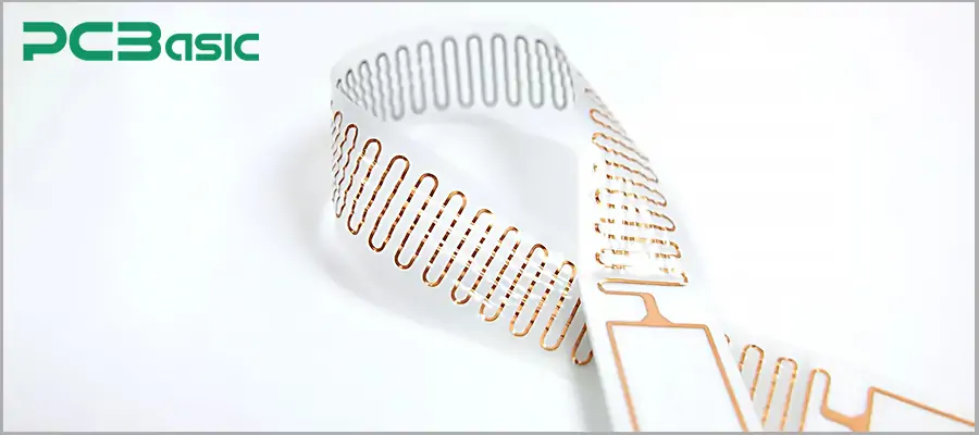
Transparent PCBs are one of the most modern inventions in the electronics industry, where the internal circuit can be seen through the boards due to their transparency. This type of transparency can be achieved with materials such as glass, polyimide, and ceramics which permit high optical transmissivity. You can find more and more applications of transparent PCBs in high technology, such as medical devices, consumer electronics, and 5G communication technology.
After reading this article, you will gain a basic understanding of the materials, types, and production methods of transparent PCBs and how they elevate industries to the next level. This blog will help clarify the main contributions and issues and understand the significance of transparent PCBs in today's advanced technologies.
Transparent PCBs are composed of unique materials, a characteristic that enables the PCBs to be light-penetrable. Such clear PCB variants of conventional opaque PCBs create an opportunity for industries that need to inspect internally placed components or appreciate the aesthetics of the design. For instance, within LED devices and other electronic devices, it becomes beautiful if the electronic device has a glass PCB, not plastic.
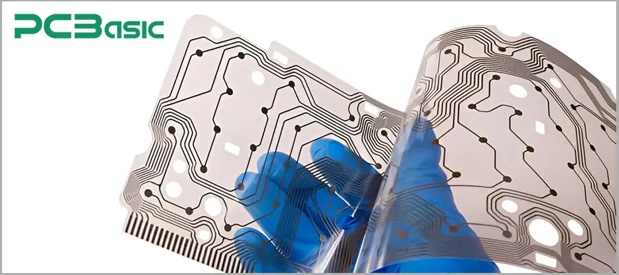
The transparent PCB doesn't compromise performance. It retains the same electrical functionalities, making it a mixture of beauty and function. The application of transparent PCB material spans various industries, including the current trends in wearables, flexible electronics, and medical devices where their flexibility, attractiveness, and sturdiness offers excellent advantages.
Transparent PCB's material composition is the most critical aspect. These materials must be chosen very carefully to achieve the required transparency, fair mechanical, and electrical properties. Here are the common transparent PCB substrates:
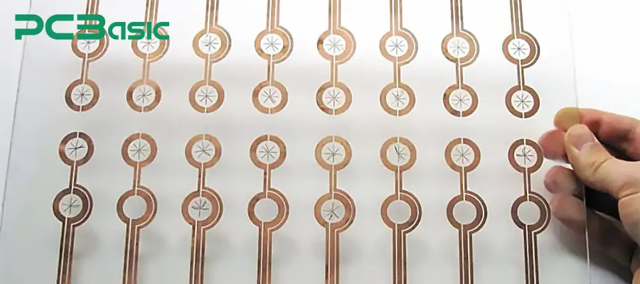
Transparent Polyimide
The flexibility and thermal stability of polyimide make it a material of choice in transparent flexible PCBs. This PCB clarity can achieve up to 95%. Due to its thin weight & soft nature, clear flexible circuit boards are formed which can be twisted & bent.
Polycarbonate (PC)
The clear PCBs use a material called polycarbonate, which is impact-resistant and has good light transmittance as well. Polycarbonate is lightweight, shockproof and can endure extreme temperatures. Because of this, polycarbonate is highly utilized in the transparent PCBs of electronic devices where ruggedness is required, such as automotive displays, consumer electronics, and also protective casing for delicate electronic parts.
Polyethylene Terephthalate (PET)
It is quite evident that Polyethylene Terephthalate (PET) is most often the chosen material for clear circuit boards due to its properties like mechanical strength and chemical resistance. PET is mostly applied in flexible printed circuits (FPCs), which require both transparency and flexibility. PET-based PCBs find application in wearables, sports gadgets, flexible displays, and pliant electronics.
Polymethyl Methacrylate (PMMA)
Also known as acrylic, PMMA has great transmission of light and can even replace glass due to its lesser weight. PMMA plastics superiority makes it suitable for widespread use in illumination systems, transparent displays, and optical devices.
Glass-Reinforced Epoxy (G10 or FR4)
Although they do not reach full transparency, the glass-reinforced epoxy polymers can be made into a transparent PCB. The mechanical strength is high, and the electrical self-insulation is good. In industrial control and LED lighting applications, glass-epoxy composites offer partial light transmission and structural support.
Liquid Crystal Polymer (LCP)
LCP is an engineering thermoplastic with exceptional performance, good electrical resistance values, and low water absorption. LCP also offers excellent chances against high-frequency signals and has the advantage of transparency, which makes its usage appropriate for high-end communication devices and medical instruments.
Transparent Circuit Boards are available in many variations based on clarity, usability, and effectiveness requirements.
Transparent Glass PCB (Glass Circuit Board):
Most electronic devices use circuit boards created from glass or sapphire, ensuring good optical clarity and strength. Construction of glass circuit boards is mainly preferred in industries where aesthetics and durability are of great concern. They are used in most applications, such as LED displays and high-end optical systems.
Ceramic Transparent Circuit Board:
These transparent PCBs use ceramics as matrix materials, including alumina or magnesia. Due to these materials having good thermal conductivity, they are suitable for high-power applications like infrared lighting, high-power LEDs, and other heat-generating devices. They are termed invisible but still present enough clarity for some optical applications in specific domains.
Transparent Flexible PCB:
Using clear polyimide or PET does not rule out the incorporation of transparent flexible PCBs. Transparent flexible PCBs have flexible and lightweight properties by using transparent polyimide or PET films. These types of PCBs are used in wearable devices and cameras and enable designers to put circuits in devices that can be bent or folded, increasing portability and design flexibility.
|
Type |
Advantages |
Disadvantages |
Applications |
|
Transparent Glass PCB |
Completely see-through, high-temperature resistance, environmentally friendly |
Fragile, higher production cost |
LED displays, solar panels, optical devices |
|
Ceramic Transparent Circuit Board |
High durability, excellent heat resistance |
Less transparent, expensive |
Infrared windows, high-power LEDs, industrial applications |
|
Transparent Flexible PCB |
Lightweight, flexible, easily adaptable |
Low thermal resistance, complex to produce |
Wearable electronics, flexible medical devices, foldable phones |
To get the required visual transparency along with functionality, designing a transparent PCB is challenging in terms of technology and materials. Here are some of the things you should consider:
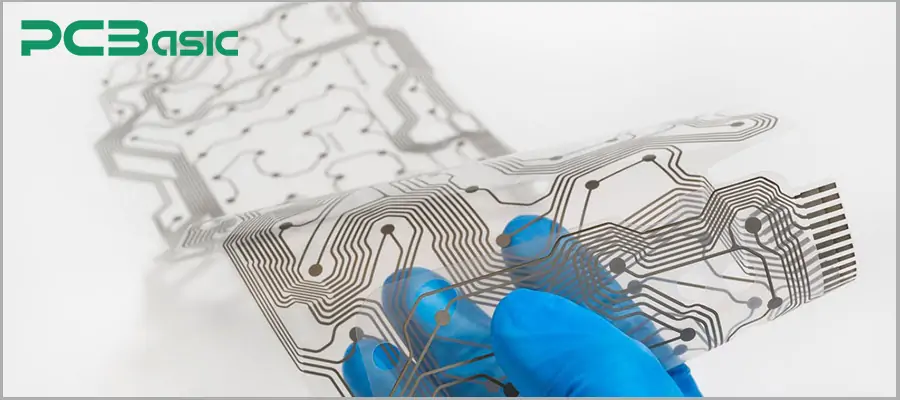
1. Material Selection
The choice of substrate material determines the heat management, optical clarity, and physical flexibility. The materials mainly used for transparent PCBs include glass, transparent polyimide, and ceramics, each with its own properties and thus being used for different applications.
2. Thermal Management
Due to materials' transparency, these generally exhibit lower thermal conductivity than more traditional PCB substrates such as FR4. Thermal management is, hence, particularly important to the design of high-power-density transparent PCBs. The engineers must include effective mechanisms for heat dissipation, particularly those involving heat sinks or thermal vias, so that heat may be properly dissipated. Otherwise, transparent PCBs are at risk of overheating, and this will reduce performance or make them fail.
3. Mechanical Stability
Transparent PCBs, especially the glass-based types of PCBs, are much more brittle than their opaque counterparts. Although glass circuit boards are extremely transparent and rigid, they are always likely to crack or shatter under mechanical stress. Designers must be able to include protective features, such as reinforcement layers or flexible supports, to ensure the board can withstand physical stress during installation and operation.
4. Manufacturing Complexity
Unlike producing conventional PCBs, making transparent PCBs involves unique processes and materials, which renders them more complex. For example, working with transparent substrates made out of glass or polyimide is more difficult than working with FR4 laminate materials. Further etching, plating, and even stacking layers of PCB has to be done precisely to maintain the transparency as well as the standard functionality of the PCB.
And in the case of clear flexible PCBs, engineers and designers face challenges when applying copper traces. Such substrates do not tend to use more than two thin copper layers, so creating a practical circuit is harder than in the case of rigid PCBs. Moreover, processes of drilling, cutting, and even laser etching become more complicated due to the nature of such substrates as glass or ceramic.
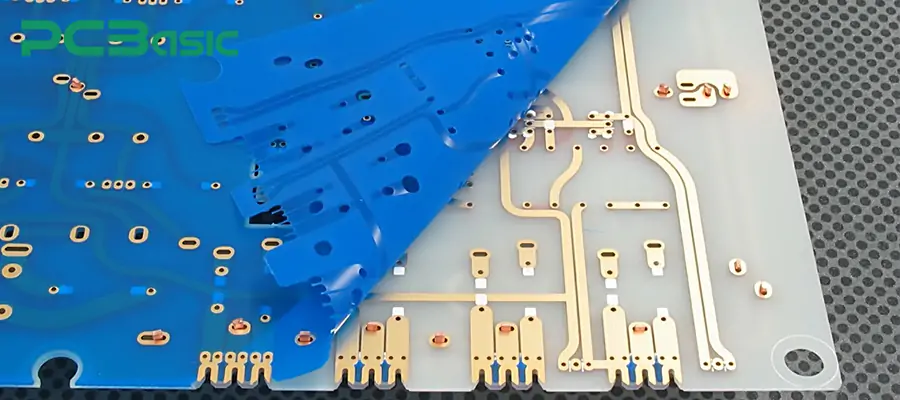
This general process includes:
Substrate Fabrication: The transparent material (for example, glass or polyimide) is processed to create the base layer of the PCB.
Copper Layer Application: Some thin copper layers are used to create conductive pathways for electrical signals across the board. One must be very cautious when applying these copper layers so that they do not compromise the clarity of the board.
Photolithography and Etching: On top of the copper layer, a photoresist layer is formed and exposed to UV light, creating a specific circuit pattern. All the undesired copper is removed, leaving only the etched spaces on the cover with the proper geometry.
Solder Mask and Surface Finishing: Solder mask, for example, immersion gold plating, is utilized during the assembly to cover up the circuits and avoid damage, as well as surface finish.
Inspection and Testing: After manufacturing the transparent PCB, engineers perform extensive additional testing of the board to validate all the requirements in terms of clarity and proper electrical behavior.
With a wealth of experience in this area, PCBasic has advanced technologies for producing aesthetically appealing and highly efficient transparent PCBs. PCBasic specializes in the domain of transparent PCB technologies to produce boards for applications in high-performance and aesthetically oriented designs. From flexible transparent PCBs to rigid glass-based designs, whether it's small-scale prototypes or large production runs, PCBasic guarantees reliability and durability in every product that comes with optical clarity.
Introducing transparent PCBs in the industry has changed the perspective of circuit board design which incorporates functional and aesthetic transparency. Their usage in advanced domains, such as wearable technology, medical devices, and high-end consumer electronics, is increasing due to the beauty and performance requirements. Trends for the rise of these PCBs lead only forward in the development of electronics and present almost endless opportunities for creativity.
 About PCBasic
Time is money in your projects – and PCBasic gets it. PCBasic is a PCB assembly company that delivers fast, flawless results every time. Our comprehensive PCB assembly services include expert engineering support at every step, ensuring top quality in every board. As a leading PCB assembly manufacturer, we provide a one-stop solution that streamlines your supply chain. Partner with our advanced PCB prototype factory for quick turnarounds and superior results you can trust.
Assembly Enquiry
Instant Quote
Phone contact

+86-755-27218592
In addition, we've prepared a Help Center. We recommend checking it before reaching out, as your question and its answer may already be clearly explained there.
Wechat Support

In addition, we've prepared a Help Center. We recommend checking it before reaching out, as your question and its answer may already be clearly explained there.
WhatsApp Support

In addition, we've prepared a Help Center. We recommend checking it before reaching out, as your question and its answer may already be clearly explained there.