Global high-mix volume high-speed PCBA manufacturer
9:00 -18:00, Mon. - Fri. (GMT+8)
9:00 -12:00, Sat. (GMT+8)
(Except Chinese public holidays)
Global high-mix volume high-speed PCBA manufacturer
9:00 -18:00, Mon. - Fri. (GMT+8)
9:00 -12:00, Sat. (GMT+8)
(Except Chinese public holidays)
HomePage > Blog > Knowledge Base > PCB X-Ray Inspection for Quality Control
In the electronic manufacturing process, the manufacturing and assembly quality of the circuit board is very important. PCBasic has always been committed to improving product quality through advanced technologies and inspection equipment, such as flying probe testing, automatic optical inspection (AOI) and PCB X-ray inspection.
Whether in the medical industry, aerospace manufacturing or consumer electronics, PCB X-ray inspection provides excellent accuracy for detecting defects in components, solder joints and inner layers. This blog will detail PCB X-ray inspection techniques, including:
• Definition and classification
• Working principles
• Advantage
• X-ray vs Other PCB Inspection Methods

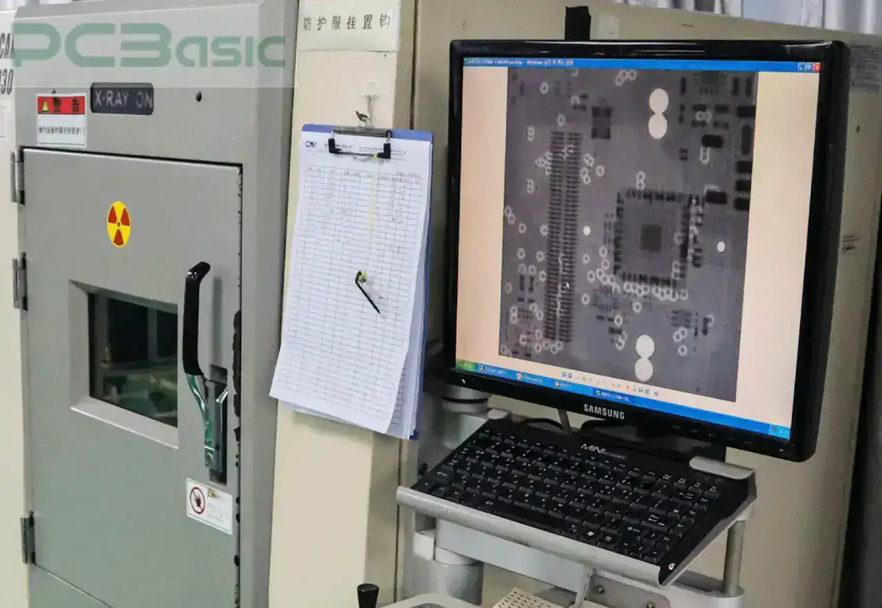
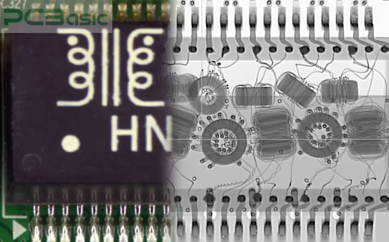
PCB X-ray inspection is an advanced non-destructive testing technology, which can use X-ray to check the internal structure of circuit boards or PCB components without disassembling them. Visual inspection can only identify surface defects; whereas X-ray inspection can reveal hidden defects as it has the ability to penetrate solder joints, components, and even internal layers. This method is known to be best for testing more intricate components such as the Ball Grid Array (BGA) chips and helps in stabilizing and ratifying the internal structure of PCBs.
For different functions and applications, PCB X-ray inspection machines also have different types. Common PCB X-ray inspection machines are 2D X-ray machines, 3D X-ray machines and automated X-ray inspection systems (AXI).
|
Type |
Function |
Advantages |
|
2D X-ray Machine |
Surface-level inspection, checking solder joints and component placement, basic quality control. |
Simple operation, low cost, suitable for routine checks. |
|
3D X-ray Machine |
Generating 3D cross-sectional images for analyzing solder joints and internal layers. |
High precision, detects hidden defects, suitable for complex analysis. |
|
Automated X-ray Inspection System (AXI) |
High-speed, large-scale automated inspection, widely used aerospace manufacturing and large-scale electronics production. |
High efficiency, suitable for mass production, automatically detects defects. |
A PCB X-ray inspection machine itself includes several essential components:
X-ray Source: Produces the X-rays used to scan the circuit board.
Detector: Used for capturing the X-ray image and indicates the areas that suspects defects might appear.
Manipulator System: Moves the PCB to ensure all regions are inspected.
Software: Analyzes the data captured and gives insights for quality assessment.
Today, modern automated X-ray inspection systems are equipped with advanced AI algorithm boosting detection accuracy and minimizing human errors, making them hardly replaceable in electronics manufacturing industries, and production of medical devices.

First, the staff put the circuit board into a PCB X-ray inspection machine, and after the device is started, the system will automatically start scanning the circuit board and prepare for the inspection process.
X-ray Penetration:
The device then uses X-rays to penetrate the circuit board and capture a photographic image of the inside of the board, looking at solder joints, components and any internal defects that may exist.
Image Processing:
Next, the detection system analyzes the captured X-ray images through advanced image processing algorithms. These algorithms can automatically identify problems on the board, such as solder joints, components, and potential defects.
Reporting:
Finally, the system will generate a detailed inspection report based on the analysis results. The report lists all problems found, helping engineers quickly locate and resolve defects to ensure product quality.
In the circuit board production and assembly process, reliable PCB manufacturers such as PCBaisc usually use a series of inspection methods to ensure product quality. Different inspection technologies can help detect various defects in the circuit board, such as poor soldering, component misalignment, short circuit, open circuit, etc. In the table below, let’s compare several common PCB inspection techniques, including X-ray inspection, functional testing, flying probe testing and Automated Optical inspection (AOI), and compare the PCB defects that each inspection method can detect.
|
Defect Name |
X-ray Inspection |
Functional Testing |
Flying Probe Testing |
AOI |
|
Soldering Defects |
Yes |
No |
Yes |
Yes |
|
Component Misalignment |
Yes |
No |
No |
Yes |
|
Open Circuit |
Yes |
No |
Yes |
No |
|
Short Circuit |
Yes |
No |
Yes |
No |
|
Voids |
Yes |
No |
No |
No |
|
Excessive Solder |
Yes |
No |
No |
No |
|
Incomplete Solder Joints |
No |
No |
No |
Yes |
|
Missing Components |
No |
No |
No |
Yes |
|
Cold Solder Joints |
No |
No |
No |
Yes |
|
Functionality Issues |
No |
Yes |
No |
No |
|
Signal Loss |
No |
Yes |
No |
No |
|
Component Failure |
No |
Yes |
No |
No |
PCB X-ray inspection stands out as an indispensable tool for ensuring quality control in modern electronics manufacturing. PCBasic invested in reliable automated X-ray inspection machines not only to detect defects, but also to protect its brand reputation in an industry that demands high precision. Choose PCBasic as your PCB or PCBA manufacturer to ensure the quality of your products by using a range of advanced inspection technologies such as PCB X-ray inspection.

Assembly Enquiry
Instant Quote
Phone contact

+86-755-27218592
In addition, we've prepared a Help Center. We recommend checking it before reaching out, as your question and its answer may already be clearly explained there.
Wechat Support

In addition, we've prepared a Help Center. We recommend checking it before reaching out, as your question and its answer may already be clearly explained there.
WhatsApp Support

In addition, we've prepared a Help Center. We recommend checking it before reaching out, as your question and its answer may already be clearly explained there.