Global high-mix volume high-speed PCBA manufacturer
9:00 -18:00, Mon. - Fri. (GMT+8)
9:00 -12:00, Sat. (GMT+8)
(Except Chinese public holidays)
Global high-mix volume high-speed PCBA manufacturer
9:00 -18:00, Mon. - Fri. (GMT+8)
9:00 -12:00, Sat. (GMT+8)
(Except Chinese public holidays)
HomePage > Blog > Knowledge Base > Tooling Holes: Optimize PCB Precision and Manufacturing Efficiency
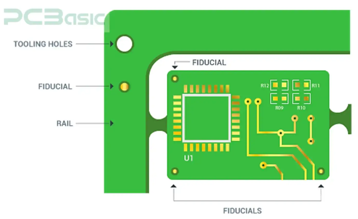
Tooling holes are the unsung heroes of PCB manufacturing — ensuring precision and alignment throughout the PCB production process. Though tiny in size, they are indispensable for PCB panel alignment, multi-layer registration and efficiency in automated processes such as fabrication assembly and automated optical inspection (AOI).
In this guide will we take an in-depth look at tooling holes: what they are, their significance, and how to design them for the best results possible!
Tooling holes, or alternatively, alignment holes or mounting hardware, are pre-drilled holes to secure and align the PCBs as per the need during the manufacturing and assembly process. These holes create well-defined reference points, which guarantee same positioning and correct registration across processes such as:
• Drilling
• Layer Registration
• Stencil Alignment
• Component Placement
Without tooling holes, the fabrication assembly process could face misalignment issues, impacting copper pour connections and overall board quality.

There are some advantages of tooling holes that help the production of PCBs:
1. Precise Alignment
For multi-layer PCBs, tooling holes align the different layers of bare PCBs, ensuring that the layers line up making it impossible for the traces to short with one another.
2. Stability During Assembly
Tooling holes are used to locate and secure PCBs on machines like AOI machines and pick-and-place equipment, ensuring accurate board connection and the placement of components on the board.
3. Improved Yield
When PCBs are aligned adequately, it leads to decreased defects, which allows them to pass inspection criterion and be qualified for quality standards.
4. Facilitates Automated Processes
Tooling holes are essential for aligning a PCB panel before it is fed automatically through a machine to apply solder paste, or even for an automated optical inspection of the panel.

PCB tooling holes and mounting hole are two different terms needed to clarify their differences in precise PCB design and practice in PCB assembly.
• Tooling Holes:
Used during manufacturing to align and secure the PCB. These are temporary and typically not part of the final product.
• Mounting Holes:
Designed for securing the PCB to an enclosure or device. These are permanent and often require mounting hardware, such as screws or standoffs, to secure the board in place.
Key Differences:
• Function: Tooling holes are for manufacturing; mounting holes are for product integration.
• Placement: Tooling holes prioritize alignment; mounting holes are placed where the PCB attaches to the device.
• Design Guidelines: Mounting holes must account for environmental factors, such as vibration and thermal expansion, which are less relevant for tooling holes.
Let’s compare the two in a chart:
|
Aspect |
Tooling Holes |
Mounting Holes |
|
Purpose |
Align PCBs during manufacturing |
Attach PCBs to enclosures |
|
Permanence |
Temporary, removed after production |
Permanent, part of the final product |
|
Placement |
For alignment and layer registration |
At mounting points in the housing |
|
Design Focus |
Alignment and equipment compatibility |
Vibration and structural support |
|
Hardware |
No additional hardware needed |
Requires screws or standoffs |
There are a few basic guidelines to keep in mind to get the most out of tooling holes:
1. Symmetrical Placement
Keep all tooling holes for the PCB center symmetric to prevent PCB from bending out of balance and getting unstable in handling.
2. Maintain Edge Clearance
Don't make structural invalidations by placing tooling holes less than 3-5mm from the PCB edge.
3. Avoid Critical Areas
To avoid interference with the electrical circuit, do not place tooling holes on trace, pad or copper pour regions.
4. Standardize Sizes
Use standard hole sizes like 3.0mm or 5.0mm to ensure that they are compatible with manufacturing equipment.
5. Consistent Registration
Align tooling holes across all layers of a bare PCB to ensure proper stack-up in fabrication assembly.
Tooling holes are needed for PCB alignment during automatic processes such as:
1. Pick-and-Place Assembly
Tooling holes secure the PCB in position during the placement of components, enabling precise board connection while reducing the risk of misalignment.
2. Solder Paste Stencil Alignment
Stencils used for solder paste application rely on tooling holes for proper alignment with the PCB pads.
3. Automated Optical Inspection (AOI)
Tooling holes, which are used as reference points for an AOI machine to check solder joints and component placement, enable accurate inspection
Tooling holes are an important aspect of PCB design as they increase the accuracy and efficiency of fabrication assembly. With a few basic guidelines to follow regarding how they are designed and placed, you can ensure that your PCBs can check all standards for manufacturing and quality.
1. How many tooling holes should a PCB have?
Most designs require two to four holes, depending on the PCB size and complexity.
2. Can tooling holes be used for mounting?
While tooling holes are temporary, they can double as mounting holes if designed and positioned appropriately.
3. What is the standard size for tooling holes?
Common sizes are 3.0mm or 5.0mm, but you should always consult your manufacturer for specific requirements.
4. Are tooling holes necessary for single-layer PCBs?
While not always mandatory, tooling holes improve alignment and assembly accuracy, even in simple single-layer designs.

Assembly Enquiry
Instant Quote
Phone contact

+86-755-27218592
In addition, we've prepared a Help Center. We recommend checking it before reaching out, as your question and its answer may already be clearly explained there.
Wechat Support

In addition, we've prepared a Help Center. We recommend checking it before reaching out, as your question and its answer may already be clearly explained there.
WhatsApp Support

In addition, we've prepared a Help Center. We recommend checking it before reaching out, as your question and its answer may already be clearly explained there.