
Global high-mix volume high-speed PCBA manufacturer
9:00 -18:00, Mon. - Fri. (GMT+8)
9:00 -12:00, Sat. (GMT+8)
(Except Chinese public holidays)





HomePage > Blog > Knowledge Base > Optical Sensor PCB Assembly: What to Check Before Production
1. Define the Optical Sensor Board and Assembly Scope
2. Review Components, Files, and Mechanical Requirements for an Optical Sensor PCB
3. Plan Soldering, Sensor Handling, and Optical Surface Protection
4. Agree on Inspection, Optical Sensor Testing, and Calibration
5. Confirm Supplier Readiness Before Releasing Optical Sensor PCB Assembly Production
A sensor board that reads perfectly on the
bench can drift in the field for reasons that have little to do with the
design. A smear of flux on the window, a part reflowed past its limit, or a
lens scratched during packing can be enough to affect performance. Optical
sensor PCB assembly leaves little room for these slips than most boards do,
because the optical surface is part of the product.
Demand for optical sensors continues to grow. According to Global Market Insights, the optical sensors market is expected to grow from USD 29.5 billion in 2026 to USD 71.7 billion by 2035 at a 10.4% CAGR. Many of those sensors end up on an optical sensor PCB that someone has to build, handle, and test consistently.
This article explains what to check before production starts, from PCB requirements and component selection to design files, soldering, and handling. It also includes the inspection, test, and calibration process used to evaluate performance, as well as the selection of the right supplier.
Before requesting a quote or starting production, the team needs to agree on the board's requirements. Optical sensor board assembly can vary depending on the type of sensor and the product it will be used in.
An optical sensor PCB assembly includes the sensing device itself, which could be a photodiode, ambient light sensor, proximity sensor, or optical encoder sensor. It may also have supporting components such as an amplifier or converter, a microcontroller, or interface power circuitry, and connectors.
Some boards have both the light source and detectors. The light source may be an LED or laser diode. In other cases, the boards hold the electronics, and the lens, light pipe, or housing is fitted later.
This difference also affects production requirements. An assembled optical sensor board without integrated optics needs different assembly instructions and tests than a complete sensor module. You may need a different supplier for a complete sensor module than for board-level assembly.
Discrete optical sensors, image sensors, and optical communication modules are used for different things. Their assembly requirements are also not the same.
A reflective sensor arrangement could have an emitter located near the detector on the circuit board. While one design would detect reflected light off an object, another would position both the emitter and the detector opposite each other across a sensing gap. An imaging sensor may require a lens holder, while dust on the optical components can influence the picture quality. Optical communication modules may use optical fibers and connectors for fast data transfer.
Since different components require different handling and testing techniques, it is preferable to notify the supplier about the product to be assembled before getting the quote.

Some optical sensor PCB issues can be traced back to small errors or omissions in the files that are provided to the manufacturing facility. For an optical sensor board assembly process, it is important for manufacturers to know what the optical sensor is meant to detect or measure and the purpose of the sensor.
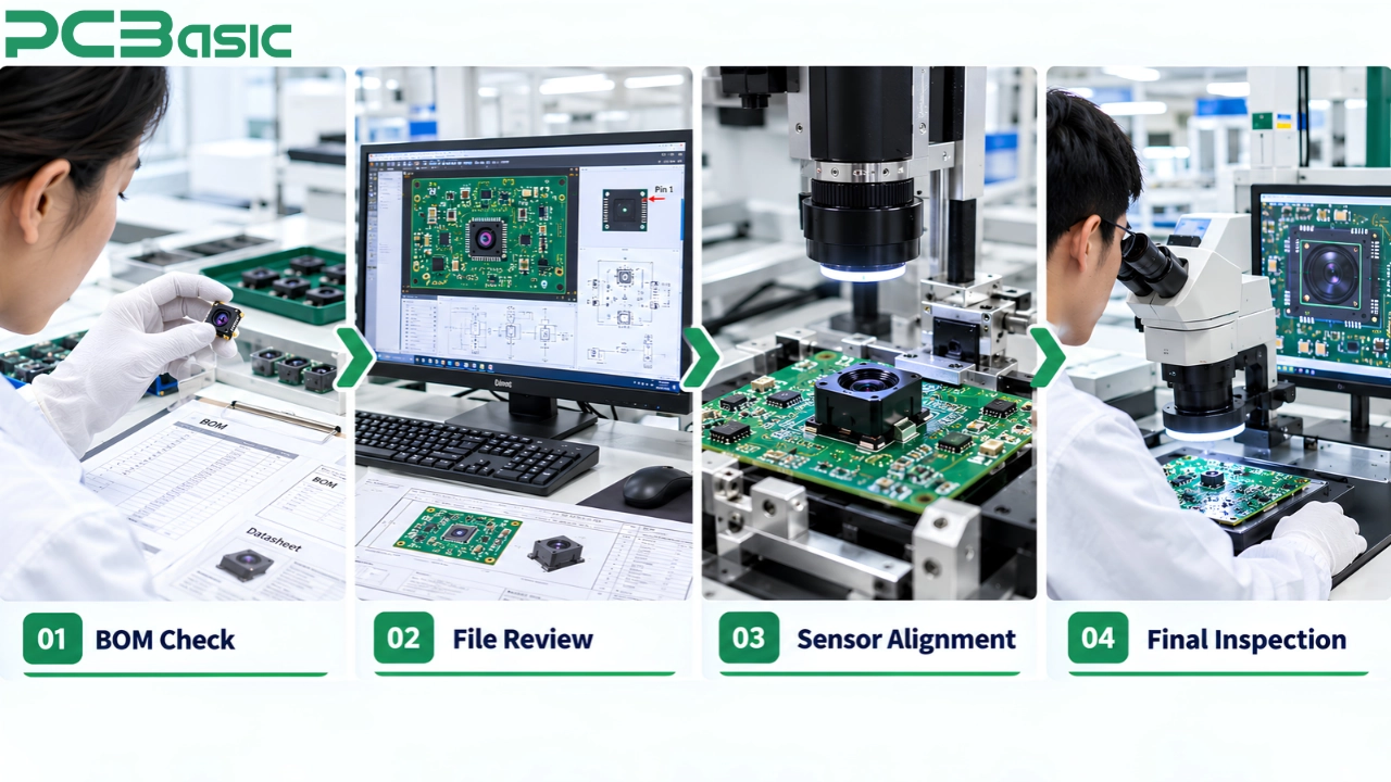
Start with the full part number, including its suffixes. Two optical sensors may look similar but still differ in spectral range, field of view, window, or package. A part can pass inspection and still turn out to be unsuitable for the product.
Check the approved BOM and list any alternatives that the team has agreed to use. PCBasic checks incoming components against the BOM before they reach the production line.
The next step is to check the production files against one another. The PCB file, placement file, and assembly drawing need to be consistent on pin-one identification where applicable, component orientation, and component positioning.
The drawings should also include information about protecting an optical sensor PCBA – protective film, including when it must remain in place or be removed, keep-out zones around the window, and restrictions regarding flux or cleaning. A note that only exists in an email chain may not reach the production floor.
The sensor's optical position matters relative to what it looks through or at, whether a window, a lens, a light pipe, or a target. The requirement should come from the product design, not from a general rule.
Some products place the sensor on its pads with standard SMT accuracy and let a housing do the rest. Others need tighter control of height or angle, and a few use active alignment. State which applies, give any limit as a number from the design, and name the datum it refers to.
This is where an optical sensor PCB assembly project most often can go wrong, and it is also where clear instructions can help prevent problems.
The device documentation sets the rules. Moisture sensitivity level, storage and baking, peak reflow temperature, and the allowed number of reflow passes all come from the manufacturer, and some optical packages add limits of their own.
Sensor handling instructions in the datasheet or application note override a shop's default process. When the two conflict, the device documentation wins, and the work instruction should say so.
Flux residue, fingerprints, and dust on an optical window change what the sensor sees. Cleaning is not always the fix, since some devices restrict water washing or ultrasonic cleaning, and a harsh solvent can cloud a window.
Conformal coating needs the same care. Mask the optical surface or define a coating exclusion area, and keep protective film in place only for the process stages permitted by the device documentation.
Later steps can undo earlier care. An adhesive that outgasses can fog an optical surface, a rework pass adds heat the sensor may not tolerate, and a loose tray lets windows touch.
Decide in advance how many reflow or rework cycles a sensor may see within the manufacturer’s limits, who approves rework, and how boards are packed so that no window contacts another surface. Light shields and lens holders add their own fit and cleanliness checks. The table below turns these points into a simple checklist.
|
Production Step |
Risk to Check |
Required Instruction |
|
Storage and baking |
Moisture absorbed before reflow |
Follow the part's moisture-sensitivity and baking instructions |
|
Reflow soldering |
Exceeding the sensor's temperature or pass-count limit |
Use the profile and limits stated in the device documentation |
|
Cleaning |
Solvent, water, or ultrasonic damage to the optical window |
Use only methods the device documentation allows, or use a validated no-clean process where permitted |
|
Conformal coating |
Coating over the optical surface |
Mask the window or define a coating exclusion area |
|
Handling and rework |
Fingerprints, scratches, repeated heat |
Define handling tools, rework limits, and who approves rework |
|
Packing |
Window contact, static, dust |
Specify trays, separators, and approved protective covers or film where applicable |
PCBasic turns agreed points like these into written work instructions, confirms them on a first article, and records each lot in MES. That documented process control helps keep the hundredth board built the same way as the first.
Testing is where an optical sensor PCBA proves its value, and it is also where hidden assumptions cause the most disputes.
Inspection checks the build. SPI and AOI show whether paste, placement, and visible joints look right, and X-ray inspection helps when a package hides its joints, subject to any device-specific radiation limits. None of them shows whether the sensor reads correctly. On an optical sensor PCBA, keep the inspection record and the performance record separate, so a pass on one never hides a gap in the other.
A board can pass AOI and still return the wrong value. Optical sensor testing needs a stimulus, so the plan should list the build checks and the performance checks as two separate items.
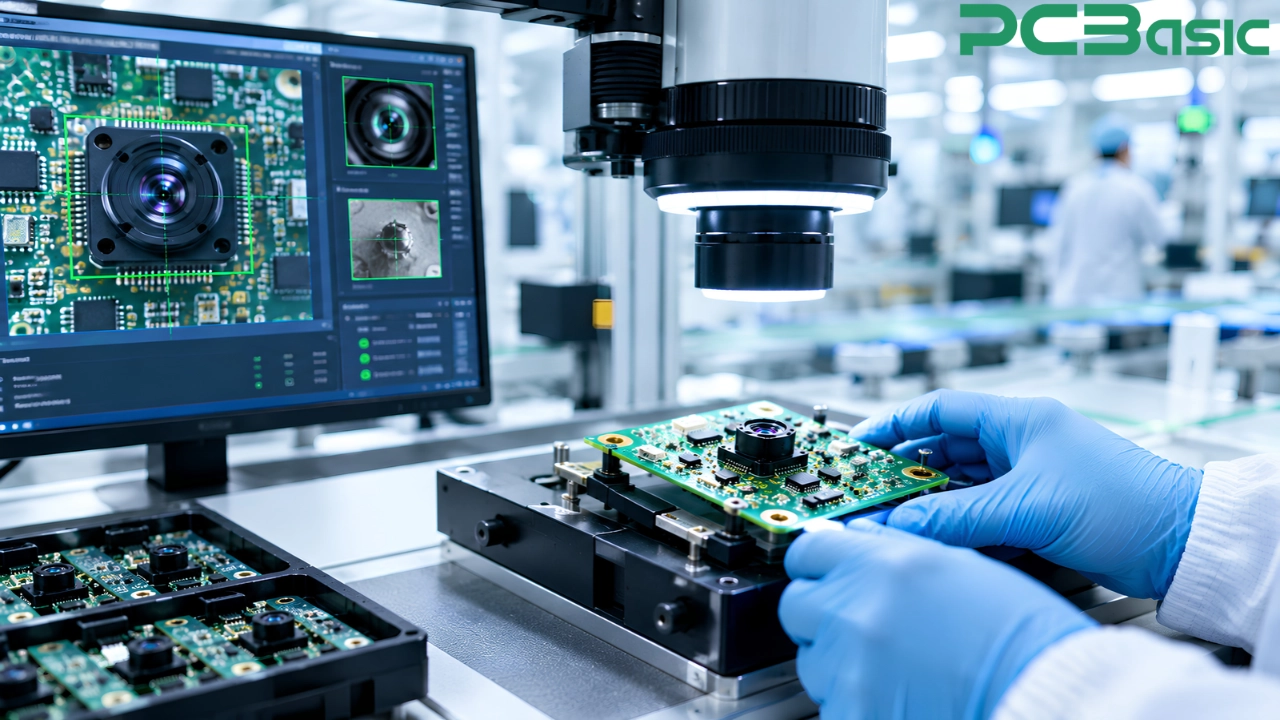
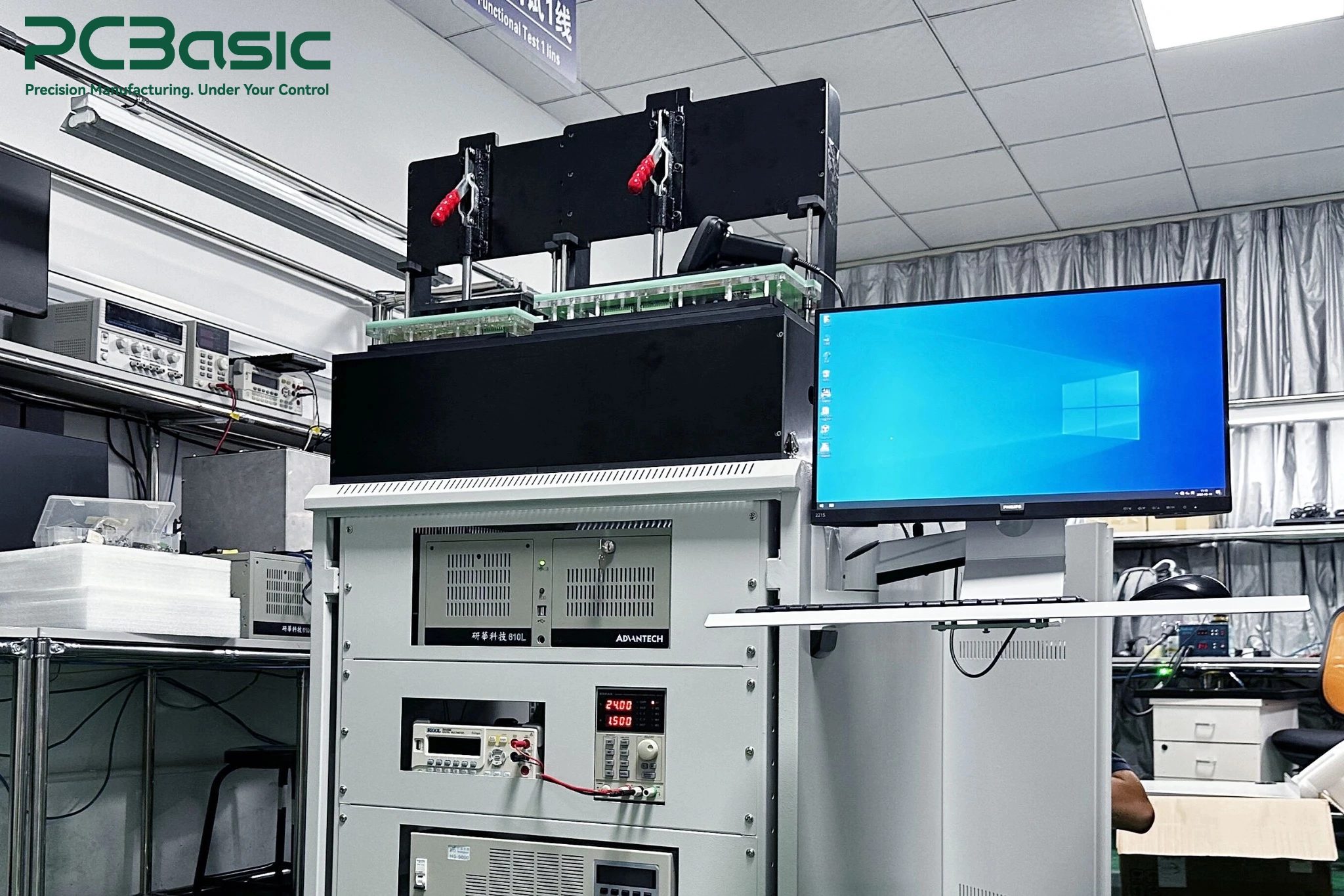
PCBA functional testing for an optical board depends on controlled conditions: the light source, the distance and angle to the sensor, the ambient light, and the reference or target. Change any of them and the readings move. A dark box or shielded fixture helps keep stray light out, so the reading more closely reflects the board's response under the specified test conditions.
Write those conditions into the test procedure, along with pass limits and the records to keep. Repeatability matters alongside measurement accuracy, since the same fixture and conditions on every unit help make results comparable from lot to lot.
Some products ship factory-calibrated, with correction values stored in memory. Others are calibrated later, inside the finished system. Both can be valid, and some projects require calibration at more than one stage.
Decide who calibrates, with what equipment, and where the values are stored. If calibration is out of scope, say so plainly. PCBasic's inspection and functional-testing capabilities work best inside an agreed project plan that states what is tested, on which fixture, to which limits, and what records come back.
A supplier can sound confident and still lack the specific experience your board needs. A few targeted questions help assess that quickly.
Ask how the supplier manages moisture-sensitive components, protects optical surfaces, and deals with rework. Ask what their inspection plan and test method would be for your sensor. See how they track their lots.
Then try the answers out on a prototype. A prototype PCB assembly done with real handling and testing processes tells you more than a brochure ever can, since things that are invisible on paper will pop up on the boards. Consider this a dress rehearsal of the entire process, not just a sample. Seek specific sensor PCB assembly experience.
Send it all together in a single package: production data, the validated BOM with alternatives, assembly diagrams with sensor notes, handling and finishing processes, the test procedures with parameters and limits, the scope of calibration, packing needs, and acceptance criteria, all with clearly identified consistent revision references.
Everything in a single package reduces room for misinterpretation. PCBasic can be a full turnkey PCB assembly partner through component procurement, assembly, inspections, and tests using a single agreed set of requirements. Just send us your production data and test specifications, and we'll have them reviewed based on your sensor and product.
Optical sensor PCB assembly works best when the little details in the documentation have been defined before the first board has been made. A scope definition, approved BOM, special handling for the devices, controlled testing conditions, and a decision on whether and where to calibrate all help safeguard optical performance and measurement reliability.
PCBasic can handle optical sensor programs through incoming material checks, documented work instructions, assembly, inspection, and functional testing. If your next optical sensor board is ready for review, send us the files and test specifications, and we will take you through it.
Q1: What is optical sensor PCB assembly?
It is the process of building boards that carry an optical sensing device and its supporting circuitry, with extra control over handling, cleanliness, and testing because the optical surface affects performance.
Q2: Are discrete optical sensors, image sensors, and optical communication modules built the same way?
No. Each has different handling rules, test setups, and mechanical needs, so the exact arrangement should be defined before anyone quotes or builds.
Q3: Does every optical sensor need active optical alignment?
No. Many boards place the sensor with standard SMT accuracy and rely on a housing, while others need tighter control, so the product design should state the requirement.
Q4: Why can an optical sensor board pass inspection and still fail in use?
Inspection checks assembly quality, but optical performance requires PCBA functional testing under defined optical and operating conditions to verify whether the sensor reads correctly.
Q5: What should a manufacturing package include for an optical sensor board?
Include production files, the approved BOM, assembly drawings with sensor notes, handling and coating instructions, the test procedure, calibration scope, packaging requirements, and acceptance criteria.

Assembly Enquiry
Instant Quote


Phone contact

+86-755-27218592
In addition, we've prepared a Help Center. We recommend checking it before reaching out, as your question and its answer may already be clearly explained there.
Wechat Support

In addition, we've prepared a Help Center. We recommend checking it before reaching out, as your question and its answer may already be clearly explained there.
WhatsApp Support

In addition, we've prepared a Help Center. We recommend checking it before reaching out, as your question and its answer may already be clearly explained there.
