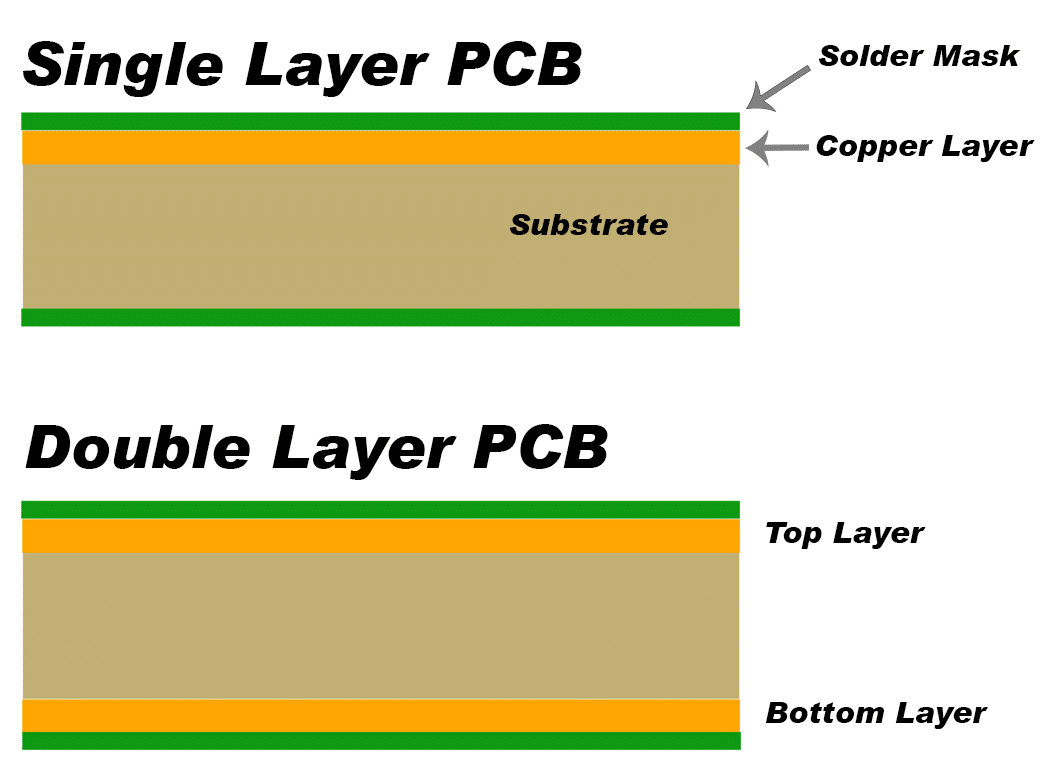
Double-sided printed circuit boards (PCBs) represent a crucial electronic design and manufacturing advancement. These versatile boards, also known as double-layer or dual-layer PCBs, play a vital role in the intricate world of electronics by providing a platform for more complex and compact circuitry.
Unlike their single-sided counterparts, double-sided PCBs offer a layering design that facilitates the integration of many components, enhancing electronic devices' overall functionality and efficiency. So, let's delve into the intricacies of double-sided PCBs, uncovering their significance, applications, and innovative technologies that propel them to the forefront of modern electronic engineering.
How are Double-Sided PCBs Made?
The process of making PCBs is intricate. After a few processes, the raw board becomes a double-sided PCB. So, brace yourself as we walk you through the double-sided PCB manufacturing process steps.
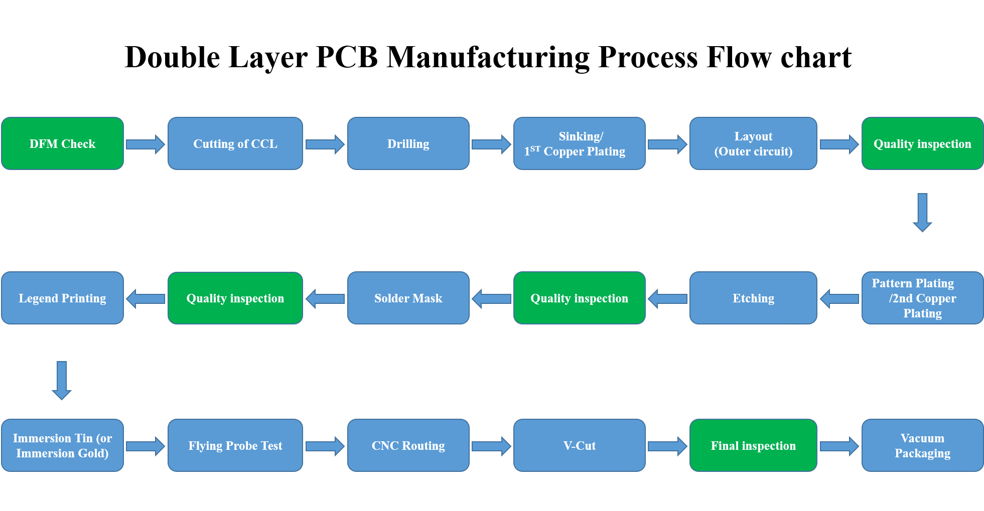
Step 1: Circuit Design for PCBs
It all starts with schematic diagram design followed by PCB design. In this process, numerous PCB design programs are selected.
Step 2: Design of PCB Layout
Once you finish the main design, you can begin designing the PCB layout. Then, print the PCB plan on glossy paper with a laser printer. However, remember to mirror the top layer layout's picture before printing the top layer. Otherwise, your circuit will be inverted.
Step 3: Materials selection for PCBs
Next, you need to select the material that best fits your needs. Certain materials and brands have distinct qualities, so choose the one that matches your layout design. For instance, if you opt for a flame-resistant board, you can use Fr-4 since it is a commonly used PCB base substrate.
However, when choosing a high-speed and high-frequency PCB, we suggest not using Fr-4 because it is inappropriate. In this regard, you can select high-frequency materials, including the RT5000/6000 series from Rogers, the TLX series from Tacanic, etc.
Step 4: Cutting of CCL(Copper Clad Laminate)
The process begins with cutting copper-clad laminate (CCL) sheets to the required size. CCL consists of a thin layer of copper foil laminated onto a non-conductive substrate. Precision in cutting ensures the proper dimensions for the upcoming steps.
Step 5: Drilling
Precise holes are drilled into the CCL to create the locations for vias and component holes. These holes are strategically placed according to the circuit design and will later facilitate the connection between the top and bottom layers of the PCB.
Step 6: Electroless Copper Deposition - Plating Through Holes
The drilled holes undergo electroless copper deposition. This involves coating the holes' interior with a thin layer of copper, creating a conductive pathway between the top and bottom layers. This process is crucial for establishing electrical connections in the final PCB.
Step 7: Photo Imaging and Printing of Circuit
A photoresist material is applied to the surface of the CCL. The circuit pattern is then printed onto the photoresist using a UV light-sensitive mask. Areas exposed to light undergo a chemical change, creating the pattern for the subsequent etching process.
Step 8: Pattern Plating
A thin layer of copper is electroplated onto the exposed areas of the CCL, reinforcing the circuit pattern. This additional copper layer enhances the conductivity of the traces and prepares the board for the next steps.
Step 9: Developing and Etching
In the "Developing and Etching" phase of double-sided PCB fabrication, precision and chemical processes combine to refine the intricate circuit pattern on the copper-clad laminate (CCL). Following the pattern plating, which involves electroplating an additional copper layer onto the exposed areas, the board is coated with a photoresist material.
This photoresist serves as a protective layer, and the subsequent steps involve exposing it to UV light through a mask that carries the negative image of the desired circuit pattern. The UV light induces a chemical change in the photoresist in the exposed areas.
Etching requires immersing the board in an acidic solution like ferric chloride. This solution chemically dissolves bare copper, leaving only photoresist-covered circuit traces and pads. After finishing, the board is thoroughly rinsed to remove etchant. Remove the developed photoresist to reveal the etched circuit pattern.
Step 10: Automatic Optical Inspection (AOI)
Next is Automatic Optical Inspection (AOI), a sophisticated quality control measure that ensures product precision and reliability. After the circuit pattern is etched onto the copper-clad laminate (CCL), the PCB undergoes AOI, a crucial optical inspection using modern technology.
A computer-controlled system with high-resolution cameras takes detailed photos of the PCB surface during AOI. Next, powerful pattern recognition algorithms analyze these photographs. The AOI program systematically detects circuit pattern discrepancies by comparing collected images to intended design parameters.
Step 11: Flying Probe Test
PCB manufacture requires testing to ensure proper operation. There may be short circuits, open circuits, or other difficulties. Thus, before shipping, the PCB must be checked. For this, use the Flying Probe Test, in which current passes through probes over connections. It tests the circuit's functionality. If probes are linked to two routes without a connection, the current should not pass. Once the test is passed, you're good to go with the PCB.
Features and Benefits of Double-Sided PCBs
Here are some of the advantages of double-sided PCBs:
Higher Density of Components
One of the best things about a double-sided PCB is that you can put parts on both sides, which makes the board twice as valuable. This makes cramming more circuitry and electronic parts into a small area possible. Ensuring maximum component density is crucial for goods that require tiny size and miniaturization, such as wearables and mobile devices. Moreover, a double-sided PCB's two-sided structure optimizes the layout for compact product footprints and density.
Additional Routing Choices
When a double-sided PCB has vias and traces on both layers, designers have more options for joining components. One side can route high-speed or crucial communications, while the other can be used for less critical traces. Additionally, specialized roles, such as ground planes or power distribution, can be allocated to the top and bottom layers.
Improved Signal Accuracy
Signal integrity is the preservation of signal strength and quality during PCB propagation. Run a continuous ground plane on the bottom layer for optimal reference grounding of signals on the top layer of a double-sided board. This guarantees that communications remain intact and offers improved isolation against noise interference. Strong ground planes are essential for high-frequency designs.
Enhanced Optimization of Layout
Placing components and routing lines on both sides allows for a highly optimized double-sided PCB layout. It is possible to arrange components and circuitry to reduce wire lengths, lessen interference between traces, and adhere to emission regulations. Additionally, it is possible to divide the board's dense areas intelligently between the sides.
Applications of Double-Sided PCB Boards
Since double-sided PCBs are affordable and capable of handling intricate circuitry, they are frequently utilized. These PCBs can be found in appliances like LED lighting and juicer machines.
Moreover, advanced power applications like converters, inverters, UPSs, and power supplies also use these PCBs. As we all know, there is a rise in demand for renewable energy, making the double-sided PCBs the talk of the town. So, let's look at some of the applications of double-sided PCBs:
● UPS systems
● Power supplies
● HVAC
● Converters
● LED lighting
● Regulators
● Phone systems
● Hard drives
● Printers
● Amplifiers
● Automotive dashboards
These are just a few examples. You can find them easily in your daily routine devices.
Single-Sided vs. Double-Sided vs Multilayer PCBs
Here's a simple chart to help you understand the fundamental difference between single vs. double-sided vs. multilayer PCBs:
|
Feature
|
Single-Sided PCB
|
Double-Sided PCB
|
Multilayer PCB
|
|
Definition
|
PCB with one layer of conducting material
|
PCB with two layers of conducting material
|
PCB with three or more layers of conducting material
|
|
Construction
|
One side for conducting material, and the other for components
|
Top and bottom layers for conducting material
|
Multiple layers of conducting material laminated
|
|
Complexity
|
Simple and basic
|
More complex than single-sided, but less than their multilayer counterparts
|
High complexity due to multiple layers and connections
|
|
Cost
|
Low cost
|
Moderate cost
|
Higher cost compared to single-sided and double-sided PCB boards
|
|
Applications
|
Camera systems, audio equipment, power supplies, calculators, solid state drives, printers, surveillance, etc.
|
LED lighting systems, vending machines, amplifiers, car dashboards, industrial controls, phone systems, etc.
|
Fiber optics, smartphones, GPS systems, scientific and space equipment, heart monitors, atomic accelerators, etc.
|
Conclusion
In conclusion, using double-sided PCBs is a big step forward in electronic design because it creates a platform that can easily combine complicated and small circuits. The production process is executed carefully, from circuit design to the final Automatic Optical Inspection (AOI) and Flying Probe Test. This makes sure that the product is accurate and reliable.
Moreover, since double-sided PCBs have benefits like more component density, routing options, and better layout optimization, they are essential in many areas, from home products to high-tech power systems.
As technology improves, double-sided PCBs play a bigger and bigger part in powering and optimizing electronic devices. This drives innovation in the ever-changing electronic engineering.