Global high-mix volume high-speed PCBA manufacturer
9:00 -18:00, Mon. - Fri. (GMT+8)
9:00 -12:00, Sat. (GMT+8)
(Except Chinese public holidays)
Global high-mix volume high-speed PCBA manufacturer
9:00 -18:00, Mon. - Fri. (GMT+8)
9:00 -12:00, Sat. (GMT+8)
(Except Chinese public holidays)
HomePage > Blog > Knowledge Base > What is AOI? | Automated Optical Inspection
AOI, or automated optical inspection, is the main part of the different manufacturing processes as well as PCB board production, where it finds any existing faults and missing components.
This process helps make high-quality products and fulfill all required parameters. It is commonly used for the automobile industry and medical instrument production since it has a high-speed process and high accuracy.
In this inspection process, the complete circuit of the PCB board is scanned, which helps to find any missing components, short circuits, or any other faults.
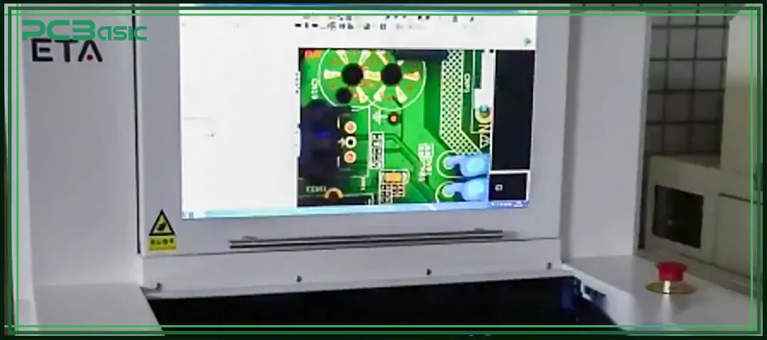
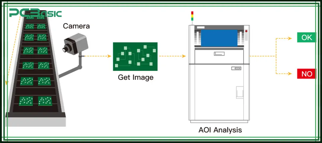
AOI stands for automated optical inspection. It is an inspection system of a PCB board that is performed at the time of manufacturing with the use of a camera that completely scans the board to find any error or missing component of the PCB board. That helps to resolve any circuit errors before the final assembly.
The basic and commonly used type of automated optical inspection system is a 2-dimensional system. In this inspection method, cameras used come with 2D features that scan the circuit in two dimensions. The main use of this process is to find errors that exist on the surface of the board, such as components not being connected accurately, faulty connections, and components not soldered accurately.
In a 2D AOI system, an image of the faulty board is taken with a camera and compared with an errorless board with proper component connections after the final circuit assembly is completed, solving the error.
The main features that help engineers use this system are their high-speed inspection, less complication during use, and low cost, which are also the main factors.
3D is the latest technique compared to the 2D system, and it uses two main methods for finding faults: laser triangulation and structured light projection.
1. For laser triangulation, a laser line is configured on the product or circuit in line, and then cameras help to record an image of the line. If there is a change in the dimension of lines, it helps to find inaccuracy on the surface. The outcomes of this process are very accurate and find height values up to one micron. But it is a slow process.
2. Structured light projections are a high-speed process compared to laser triangulation and can record a height resolution of about ten microns. This process directs light on the circuit or product and then records the results of a distorted design. The findings of distorted patterns or designs provide the height of the surface.
 About PCBasic
Time is money in your projects – and PCBasic gets it. PCBasic is a PCB assembly company that delivers fast, flawless results every time. Our comprehensive PCB assembly services include expert engineering support at every step, ensuring top quality in every board. As a leading PCB assembly manufacturer, we provide a one-stop solution that streamlines your supply chain. Partner with our advanced PCB prototype factory for quick turnarounds and superior results you can trust.
Accurate results
· There are high-resolution cameras and the latest software used in the AOI process that provide quality and errorless results.
High-Speed operations
· The working of this process is performed with speed, takes less time than other methods, finds faults in a short time, and provides results quickly.
Optimization
· AOI provides an accurate, optimized process since it builds customers' trust by reducing the chances of errors and cost-effective features.
No or less damage
· The working process of this technique is so safe that it can be easily performed without any damage to the board or affecting quality.
Low-cost process
· This method provides a detailed fault-finding process that helps to control extra costs for affected components of any circuit. It is also beneficial for PCB manufacturers to build trust in their customers and increase their sales.
Low Downtime
· This process also reduces lead time by providing detailed features of boards and faulty components in a short time and assures delivery to users.
Flexibility
· Another advantage of this process is that we can use it at any time in the PCB manufacturing process to find faults and defects. So it is mostly used after reflow soldering to find faults and damage in the soldering process and helps reduce extra expenses. It also helps to make any changes required in the assembly or manufacturing process according to the requirements of the final assembly.
· The instruments and devices used for the AOI process are complex and need trained staff and proper training to perform this test. So, it is not easy for any unskilled person to operate this apparatus.
· If new variations and changes are made in any process, then it is difficult for AOI instruments to adapt according to those changes. It is based on current working features and constantly works based on those features. That limited its use for the latest modifications.
· The AOI needed certain types of programs to work accurately, and for new processes, it may need programming according to that process. So, changes are made in the program according to process demand.
· Another limitation is that we cannot find errors other than those directed to be found. If we let the program find a mistake on the surface, it will find that error, and some other unexpected errors will not be affected by this system.
The light source, or LED bulb, is configured on AOI machines to glow the circuit board or any product. To provide 3D vision, lights follow different angles and paths to reach the circuit board. In older AOI machines, infrared and UV lights were used for glowing products; now LED lights are used on machines. The LED lights help to show different color combinations.
There are cameras installed on machines that take images of the board, and by analyzing the images, we can detect faults.
Some machines come with more than one camera for a detailed view. These connected cameras work based on programming instructions. The result of the image or resolution is the main factor for finding errors. So, use machines that are high resolution and help to get accurate results in a short time.
The central part of AOI machines working is AOI lenses that take board images in light form. After that, the image sensor is converted into an output image. This image passes through a processing system, where a detailed inspection is performed. In simple words, we can say that the workings of AOI are mostly based on lenses. So if there is a high-power lens used, it will provide clear results.
The complete working of the AOI machine is based on the instructed program. So before using AOI to find faults, provide specific details of the program about the products. Normally, two methods are used for AOI machine program software: manual programming and algorithm-based programming.

AOI's main method is to find different faults in produced products and provide quality parameters for those products. The accuracy of AOI machines helps to provide high-speed electronic manufacturing for points where manual inspection is not easy to perform. AOI finds missing components, misaligned components, and other related faults in the circuit.
What does AOI stand for in electronics manufacturing? Well, this technology is used in many ways in electronics manufacturing:
Pre-Reflow Inspection:
A pre-reflow inspection was performed to find errorless PCB assembly before moving to the final process. AOI performed before reflow soldering helps to find errors in the board, such as whether components are completely connected, or if any component or symbolic representation is missed. Finding errors before reflow helps save time and extra costs for the reworking of the board.
In pre-reflow inspection, a 2D AOI system is used to check the details of the assembly process accurately. Check that the component polarity connection is accurate and that the required components exit helps to work the PCB board accurately.
Post-Reflow Inspection
The main objective for the post-reflow inspection of the PCB board is to check to find different errors such as missing components, components connected at the wrong point or direction, colder solder joints, and any solder bridge that exists on board.
Surface mount technology inspection is a process considered the main inspection technique in manufacturing. It comes with a complete PCB board and components evaluation for proper quality and workings. This process helps to find faults that occur at the time of production so they can be solved before assembly.
The main types of SMT inspections are:
· Visual Inspection:
· Automated optical inspection
· X-ray Inspection
· In-Circuit Testing
· Functional Testing
THT AOI controls the difficulties existing in automating through-hole inspection with the use of different processes such as mechanical, optical, and software design.
The inspection helps to detect if there is any solder without a pin, no solder exits, and no pin connected. It also finds the solder deficiency and solder ball detection. It is also used for land-wetting defects.
The manufacturing of PCB boards and other products needs specific inspection methods to find and solve different errors at the time of manufacturing in the board or circuit. Various processes are used for the inspection of errors on board, but the most important is the AOI, or automated inspection process, which is used for finding different faults on boards, such as any component not connected, damage, short circuit, or any other related faults. This process increases the working efficiency of products and reduces the final cost.
In the AOI process resolution, cameras are used for scanning and fault sections in the PCB board. After getting that result, manufacturers estimated the fault details and solved them according to requirements. Its simple and easy-to-use features make it prominent for different manufacturing processes and developments in industries, asking for this method to use and detect faults.
Assembly Enquiry
Instant Quote
Phone contact

+86-755-27218592
In addition, we've prepared a Help Center. We recommend checking it before reaching out, as your question and its answer may already be clearly explained there.
Wechat Support

In addition, we've prepared a Help Center. We recommend checking it before reaching out, as your question and its answer may already be clearly explained there.
WhatsApp Support

In addition, we've prepared a Help Center. We recommend checking it before reaching out, as your question and its answer may already be clearly explained there.