Global high-mix volume high-speed PCBA manufacturer
9:00 -18:00, Mon. - Fri. (GMT+8)
9:00 -12:00, Sat. (GMT+8)
(Except Chinese public holidays)
Global high-mix volume high-speed PCBA manufacturer
9:00 -18:00, Mon. - Fri. (GMT+8)
9:00 -12:00, Sat. (GMT+8)
(Except Chinese public holidays)
HomePage > Blog > Knowledge Base > Via-in-Pad | PCB Design
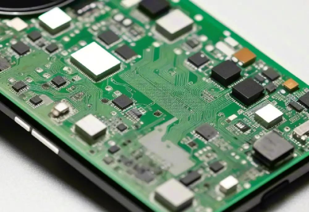
Via in pad is a technique of directly designing vias in PCB solder pads. Commonly used in high-density interconnect (HDI) PCB design, it saved space and improved the performance of circuit boards. This design allows for smaller solder joints through the board layers. In modern circuit board designs that require extremely high-density layouts, placing vias inside PCB solder pads can significantly reduce the PCB space, allowing more compact component layouts. For example:

In the PCB design of smartphones, due to significant space limitations, the use of via in pad can effectively reduce the number of PCB layers while improving the quality and speed of signal transmission.
Space saving:
The via in pad process cleverly integrates conductive holes and solder pads, greatly saving horizontal space on the circuit board. This technology perfectly fits the development trend of high-density and interconnected modern circuit boards. For modern electronic devices with high-density interconnection, this advantage is particularly prominent, as it helps to meet the design requirements of miniaturization and integration.
Signal integrity improvement:
This design shortens the path length of signal transmission, thereby reducing signal attenuation and interference during transmission. This is particularly important for high-frequency signal transmission, as it can ensure signal integrity and stability and improve the overall performance of electronic products.
Reliability Enhancement:
This technology reduces the number of connection points, thereby reducing the risk of connection failures. And it enhances the overall reliability of the circuit board, improving the durability and stability of electronic products.
Complex process:
Compared to traditional processes, the implementation process of via in pad is more complex. It requires higher technical requirements and more production steps, which may lead to an increase in production costs. Meanwhile, complex processes may also increase uncertainty and risks in the production process.
High requirements for production equipment:
Via in pad requires special production equipment and technical support. These devices usually have high technological content and cost, which may require more work to directly apply to general production lines.
Difficulty in quality control:
Via in pad's quality control also faces greater challenges. Manufacturers need to establish stricter production management and testing processes to ensure product quality and reliability.
|
|
Via in Pad |
Traditional Vias |
|
Space Utilization |
Significantly saves space. Allowing for more components and connection points to be arranged in a smaller space. |
Relatively low. Requiring more space to arrange components and connection points. |
|
Signal Integrity |
Shorter Reducing signal attenuation and interference and improving signal integrity. |
Relatively longer Be subject to more attenuation and interference. |
|
Reliability |
Enhanced the connection strength between the via and the pad, improving the reliability of the circuit board. |
Relatively low and may fail due to vibration or temperature changes.
|
|
Manufacturing Cost |
Relatively high |
Relatively low |
|
Production Cycle |
Longer |
Shorter |
|
Filler Materials |
Filled with metals (such as copper), polymers, or other composite materials. |
Usually not required. |
|
Application Scenarios |
High-density interconnect (HDI) boards, miniaturized electronic devices, and high-frequency signal transmission. |
General PCB boards, larger components, and low-frequency signal transmission scenarios |
Spacing and Layout
1. Ensure that there is sufficient spacing between the components and wiring around the via in pad to avoid interference during manufacturing and assembly processes.
2. Consider the layout of BGA and other high-density packaging to ensure that the via holes do not interfere with the placement and soldering of components.
Pad design
1. The pad size should be large enough to accommodate the via holes and provide sufficient soldering area.
2. The shape of the solder pad should be optimized according to the component type and soldering process to ensure good soldering quality and electrical connection.
Via processing
1. The via holes should be filled with appropriate filling materials (such as metal paste, polymer, etc.) to prevent solder from flowing into the holes and forming bubbles or voids during the soldering process.
2. The selection of filling materials should take into account their conductivity, thermal stability, and adhesion to solder pads.
Thermal Design and Heat Dissipation
1. In situations with high heat dissipation, careful consideration should be given to the thermal design of via in pad to ensure the reliable operation of components and PCBs.
2. Use heat sinks, heat dissipation holes, or other heat dissipation structures to enhance the heat dissipation effect.
Manufacturing and Assembly Requirements
1. Work closely with manufacturers to ensure they have the ability and experience to handle via in pad technology.
2. Follow the manufacturing and assembly guidelines provided by the manufacturer to ensure optimal quality and reliability.
The via in pad design has broad application prospects in high-density interconnect PCBs, high pin counts BGA packages, occasions with high heat dissipation requirements, and special application scenarios. However, in practical applications, it is still necessary to balance and optimize according to specific situations to ensure the best design effect.
Avoid pillow effect and bubbles
During the reflow soldering process, the air inside the via may escape due to thermal expansion, forming a pillow effect or bubbles. Therefore, it should be ensured that the through holes are fully filled and vented before welding.
Control costs and cycles
Via in pad has a relatively high cost. Therefore, this factor should be fully considered during the design phase.
Adhere to industry standards and regulations
Adhere to industry standards and specifications issued by authoritative organizations such as IPC to ensure the compliance and reliability of via in pad design.
Via-in-pad filling refers to the process of filling the via located at the solder pad. This technology can enhance the connection between the via and the pad, improving the reliability and performance of the circuit board. Here are some filling methods and materials used for filling.
§ Mechanical filling method: using specialized filling equipment to inject filling material into the via hole. This method is suitable for larger via and thicker circuit boards.
§ Chemical copper plating method: By this method, a layer of copper coating is formed on the inner wall and bottom of the vias. This method is suitable for smaller via and higher filling accuracy requirements.
§ Resin filling method: Fill conductive holes with resin or other polymer materials. This method is suitable for situations that require non-conductive filling, such as preventing electromagnetic interference (EMI) and radio frequency interference (RFI).
§ Metal filling materials: conductive metals such as copper and silver are used to improve electrical performance and connection strength.
§ Polymer filling materials: such as epoxy resin, are used for non-conductive filling to prevent electromagnetic interference and radio frequency interference while providing structural support.

§ Composite materials: Combining the advantages of metals and polymers, they have both electrical conductivity and chemical corrosion resistance.

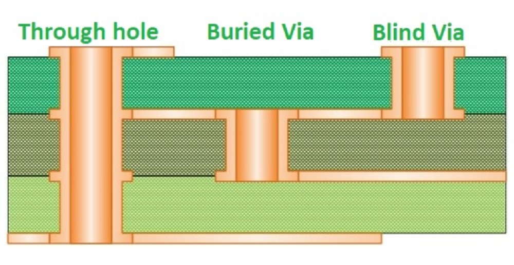
If you want to learn more about PCB vias (such as the impact of PCB vias on PCB assembly or the detailed information about the types of vias mentioned above...), please click here.
Via in pad is crucial in modern electronics. As a key PCB design innovation, it offers solutions for high-density interconnections. By directly punching vias on the solder pads and filling them with specific materials, this technology not only saves valuable space resources, but also significantly improves the integration of the circuit board and the reliability of component connections.

Assembly Enquiry
Instant Quote
Phone contact

+86-755-27218592
In addition, we've prepared a Help Center. We recommend checking it before reaching out, as your question and its answer may already be clearly explained there.
Wechat Support

In addition, we've prepared a Help Center. We recommend checking it before reaching out, as your question and its answer may already be clearly explained there.
WhatsApp Support

In addition, we've prepared a Help Center. We recommend checking it before reaching out, as your question and its answer may already be clearly explained there.