Global high-mix volume high-speed PCBA manufacturer
9:00 -18:00, Mon. - Fri. (GMT+8)
9:00 -12:00, Sat. (GMT+8)
(Except Chinese public holidays)
Global high-mix volume high-speed PCBA manufacturer
9:00 -18:00, Mon. - Fri. (GMT+8)
9:00 -12:00, Sat. (GMT+8)
(Except Chinese public holidays)
HomePage > Blog > Knowledge Base > What is a PLCC (Plastic Leaded Chip Carrier)? - PCB Package Knowledge
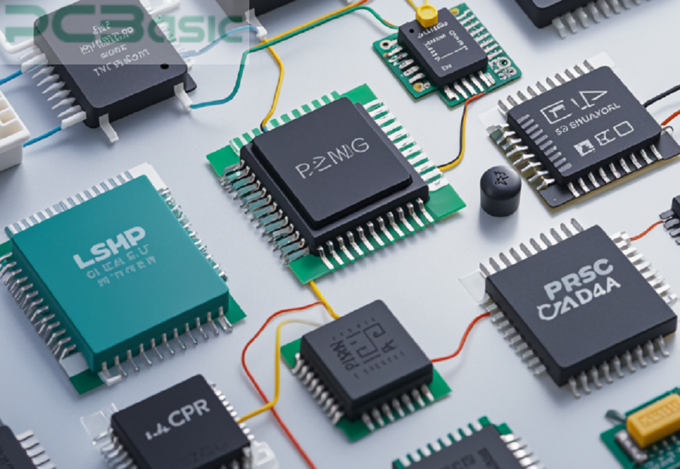
A Plastic Leaded Chip Carrier (PLCC) is a general-purpose SMT part used in many electronic assemblies. As the technology and development of PCB advanced, the trend is increasingly towards more compact and efficient chip packages, and thus the development of PLCCs.
Today, miniaturization compact solutions with high reliability and performance are of essential importance in electronics. One of these components is the plastic leaded chip carrier, abbreviated as PLCC, which is an essential component in surface mount technology, abbreviated as SMT, and is used in many electronics circuits.
With this, you will have some knowledge of the design of PLCC packages and the different types and uses. Of particular importance is that all this knowledge will not only improve your comprehension of surface-mounted devices but also point to the relevant data needed to improve PCB design in the consumer electronics industry, car manufacturing, and other applications.
The PLCC is established in planar form, often containing one or more integrated circuits to reduce the amount of space that is occupied on the PCB. A PLCC-IC package is rectangular or square and is provided with "J-leads" coming out from the corners of the package, and the component can be placed directly on the surface of the PCB.
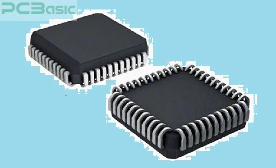
In the overall context, one of the more assignments of a PLCC package is in Surface-Mount Device (SMD) packaging. While through-hole components have to have the pins go through the defined holes in the PCB, the PLCCs can be soldered directly on the surface of the PCB. This leads to less of a requirement for making holes and thus enables the development of more compact and high-density PCB systems.
There are various types of PLCCs depending on their size and configuration for various applications.
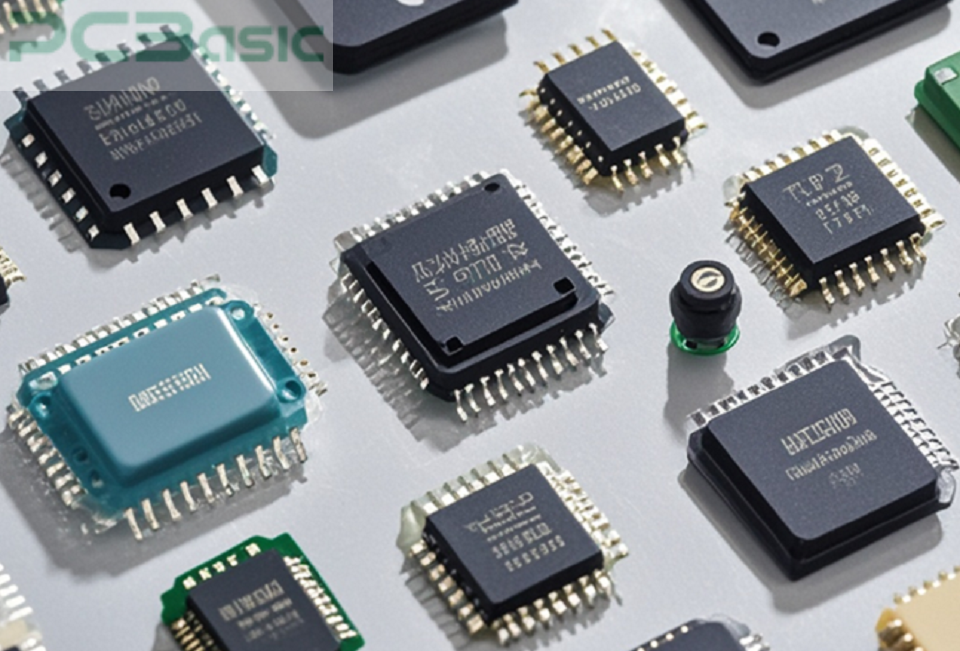
1. PLCC20: A plastic lead chip carrier with a layout of 20 pins and is most preferred in less complex or compact circuits. Due to its promising features and small size, it is suitable for devices with small spaces available.
2. PLCC28: This one comes with 28 pins, which offer more points of connection and are appropriate for somewhat more complicated gadgets.
3. PLCC44: This one has 44 pins and is widely used in intricate wiring because this option provides more contacts for connection.
4. PLCC68: A package with 68 pins used in even more complicated and high-performance products like microprocessors and memory modules.
Usage by Pin Count:
The pin count plays a direct role in the application of the PLCC. A very high pin count results in a large package size that causes a problem in the PCB area. Such devices like PLCCs, are selected by manufacturers based on the ultimate requirements of the circuit.
One of the most significant advantages of using PLCCs is that they take up less space. Since PLCCs are affixed directly on the surface of the printed circuit board, they do not require through-hole drilling, thus producing more compact printed circuit boards. Some of the common types of PLCCs include those that can be plugged into a socket.
However, there are still certain disadvantages that might be attached to the use of PLCCs. Heat dissipation is one of the most significant drawbacks of printed circuit boards and one of the most substantial limitations of PCBs. PLCCs are made of plastic mold, and their heat dissipation capability is lower compared to packages such as ceramic ones.
A PLCC package is more efficient and well-built than other packages that are used for integrated circuits. PLCCs are built with a lead frame configuration; the metal leads are curved at the end with a hook-like formation or the "J" shape that enables it to make an electrical connection to the PCB. This type of J-lead design provides a sure electrical contact and at the same time reduces the board space occupied by the component.
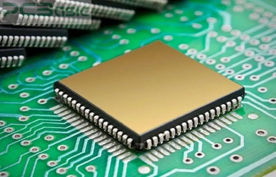
A conventional PLCC package has a square or rectangular shape, though the leads may come out from the sides of the package. The body of the PLCC is made of plastic, giving the outside case of the integrated circuit a very strong but light structure for housing its interior circuits.
The primary materials used in the construction of PLCCs include:
• Plastic: Used for the outer body as this was the most durable and cost-effective technique.
• Metal: Used for the leads and internal wiring so that it is guaranteed to carry current and signals with no problem.
These materials are selected in such a way that they possess the right combination of characteristics, such as high performance, low cost, and high reliability which makes the PLCCs ideal for a multitude of applications in the electronics industry.
This is evident after comparing the PLCCs against the LCC (Leadless Chip Carrier) package types, whereby one of the main distinguishing attributes is the leads. PLCCs (Plastic Leaded Chip Carriers) have J-shaped leads extending from the package, while LCCs are leadless, which often makes them smaller and more compact.
There is a wide market for PLCCs since they are utilized in various industries owing to their flexibility and small size. Some of the most common applications include:
Consumer Electronics: With size and performance characteristics, PLCCs are used in devices such as TVs, game consoles, and mobile phones.
Automotive Systems: Some of applications of PLCCs in car electronics which include ECUs, airbags, and infotainment modules.
Industrial Systems: Besides the PLCCs mentioned above, they are also commonly applied in industrial control equipment and sensors.
In the current electronic systems, the PLCC is an indispensable component since it is compacted and compatible with sockets, making it suitable for different industries. When aiming at designing consumer electronics, automotive systems, or industrial machinery, it is crucial to get to know the so-called PLCC package to gain some insights into efficient PCB layouts.
Assembly Enquiry
Instant Quote
Phone contact

+86-755-27218592
In addition, we've prepared a Help Center. We recommend checking it before reaching out, as your question and its answer may already be clearly explained there.
Wechat Support

In addition, we've prepared a Help Center. We recommend checking it before reaching out, as your question and its answer may already be clearly explained there.
WhatsApp Support

In addition, we've prepared a Help Center. We recommend checking it before reaching out, as your question and its answer may already be clearly explained there.