PCB trace technology is the foundation of modern electronic design. The pathways or traces in a printed circuit board (PCB) that connect the components are the PCB traces, the lifeblood of a PCB. The PCB (Printed Circuit Board) traces are a crucial part of the electronic device that impacts its reliability, functionality, and performance. In addition, it has a significant role in defining the electrical features of a circuit in engineering projects. Proper design has the ability to mitigate electromagnetic interference, improve thermal management, reduce signal loss.
Proper assembly techniques ensure these intricate traces function optimally. This guide deals with all the aspects of PCB traces. It covers the basics of PCB traces, calculations, design tips, and best practices of PCB traces whether you are a beginner or experienced engineer.

What is PCB Trace?
Trace is a thin copper conductive pathway. It is like a tiny road on a map that have guiding electrical signals where they need to go. They transfer electricity from one point to another. They link components such as integrated circuits, capacitors, and resistors. And, these parts would not communicate properly without traces. Hence the entire circuit wouldn’t not work.
Now, let’s discuss some basics of PCB trace.
Basics of PCB Traces
Being a designer or an engineer, you should know the basics of PCB traces to craft highly functional printed circuit boards. To add more, mastering basics can make efficient, advanced, and reliable electronic designs as modern technology demands. These include:
Trace Material: Copper is widely used in PCB traces because it is both an excellent conductor and cost-effective.
PCB Trace Width: It is the width of the copper path. Matching the trace width to the flowing current is important as it avoids overheating and potential failure.
PCB Trace Thickness: It is the thickness of the copper layer. The trace thickness is directly related to the current it carries.
PCB Trace Resistance: Every trace has a small resistance that combines to give the overall resistance of the circuit. And, low resistance means optimal functionality.
Routing And Spacing: Trace routing should aim to minimize the sharp turns. Because they can increase the resistance or can cause signal reflections. And, Trace spacing is also important to prevent shorts and cross-talk between the traces.
Via Connections: Vias connect the traces between different layers of a PCB.

Understanding Key Parameters of PCB Traces
Some basic knowledge of PCB traces is systematically introduced above. Now, we will give a detailed introduction to the two aspects of PCB trace thickness and PCB trace calculator.
PCB Trace Thickness
PCB trace thickness is the thickness of the copper layer that makes up the traces. That’s why, it’s also known as copper thickness or copper weight. It is typically specified in ounces per square foot (oz/ft²). Common standard PCB thicknesses are:
· 0.5 oz/ft² (17.5 μm)
· 1 oz/ft² (35 μm)
· 2 oz/ft² (70 μm)
Thicker copper allows lower resistance and higher current carrying capacity. It is commonly used for power traces and high-current applications. It can be heavier in a pocket though.
A summary table of PCB trace thickness
|
Parameter
|
Description
|
|
Definition
|
The thickness of the copper layer forming the PCB traces. Also called copper weight.
|
|
Unit of Measurement
|
Typically expressed in ounces per square foot (oz/ft²).
|
|
Common Values
|
- 0.5 oz/ft² = 17.5 μm- 1 oz/ft² = 35 μm- 2 oz/ft² = 70 μm
|
|
Function
|
Thicker copper = lower resistance and higher current-carrying capacity.
|
|
Application
|
Power traces, high-current circuits.
|
|
Trade-off
|
Increased cost and reduced flexibility with thicker copper.
|
PCB Trace Current
Direct current (DC) is used in a PCB current source to make sure there is a single current flow. PCB trace current refers to the amount of current a trace can carry safely. It differs from conventional wiring due to the constraints of trace width and copper thickness. If there is no current in any given PCB, there is no power and the components would not function well.
A summary table of PCB trace current
|
Parameter
|
Description
|
|
Definition
|
The amount of electric current that a PCB trace can safely carry.
|
|
Type of Current
|
Direct current (DC) is typically used for steady, unidirectional current flow.
|
|
Importance
|
Without proper trace current, components won’t receive power and may malfunction.
|
|
Relationship
|
Trace current capacity depends on trace width, copper thickness, and temperature rise.
|
|
Design Tools
|
Use a PCB trace current calculator or trace width calculator to determine safe limits.
|
|
Key Consideration
|
Insufficient current capacity can lead to overheating, signal degradation, or failure.
|
Function of PCB Traces
Learning functions of PCB traces is also very important. PCB trace serves as an electrical pathway connecting various parts of a PCB. Yet, they perform several other vital functions. These functions include:
· PCB traces transmit electrical signals—whether digital, analog, or high-speed—between components.
· They distribute power from the power source to different parts of the circuit.
· Ground traces connect components to the ground pins. Good trace design is important for preventing ground loops and reducing noise.
· In high-speed circuits, PCB traces help to maintain the impedance of the signal transmission path.
· Traces also help contribute to the heat dissipation. Heat-sensitive designs may have some special thermal traces or heat sinks connected to the PCB to prevent overheating.

PCB Trace Design Considerations
To ensure the functional stability and long-term reliability of the equipment, a reasonable PCB traces design is of vital importance. Whether it is power supply routing or high-speed signal routing, key parameters such as PCB trace width, copper trace thickness and current-carrying capacity must be given priority consideration. The following are some key points of PCB trace design that we have summarized:
1. Trace width and copper thickness
The width and thickness of copper trace will directly affect its ability to carry current and dissipate heat. Although thinner wiring can save space, it will increase resistance and be prone to overheating. Therefore, the standard trace width should be determined based on the current demand, copper thickness and allowable temperature rise to strike a balance between space and performance.
2. Current-carrying capacity
The traces should be reasonably designed according to the current requirements of the PCB traces to ensure that the circuit board traces do not experience voltage drop or thermal damage when operating at the designed current.
3. Resistance and Signal Integrity
The longer and thinner the trace wire is, the higher its resistance will be. It is necessary to learn to use the PCB trace resistance calculator to optimize the length, width and material of the traces in order to maintain signal integrity and reduce EMI. Because excessively high resistance not only leads to energy loss but may also cause voltage fluctuations and timing issues in high-speed circuits.
4. PCB routing calculator
Learn to use the calculator related to PCB trace. Learning to use these calculators can simplify the design process. These calculators integrate the functions of PCB trace width calculator, PCB trace current calculator and resistance estimation. With the help of these tools, we can quickly and accurately determine the wiring parameters based on electrical requirements and environmental conditions, thereby enhancing the design efficiency.

The following are some calculation formulas related to PCB trace.
PCB Trace Calculator
Different PCB trace calculators calculate the specifications of the PCB traces. These specifications include the trace width, trace current, trace resistance, and trace impedance. As mentioned below is the section explaining these calculators:
PCB Trace Width Calculator
It calculates the trace width. Following is the protocol to calculate trace width:
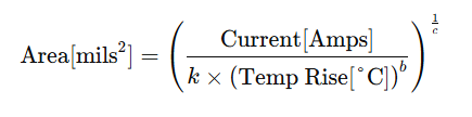
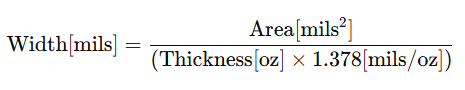
First of all, the Area is calculated by using the following formula.
Secondly, the width is calculated. The formula is given below to calculate the width.
For IPC-2221 internal layers: k = 0.024, b = 0.44, c = 0.725
For IPC-2221 external layers: k = 0.048, b = 0.44, c = 0.725
Where k, b, and c are constants resulting from curve fitting to the IPC-2221 curves. Adding more, there are multiple PCB trace width calculators available online. So, you can use any of them to calculate trace width easily.
PCB Trace Current Calculator
A PCB trace current calculator helps you to determine how much current a given PCB trace can safely carry. You can use an online trace current calculator available or follow the formulas in the IPC standards. I think, for beginners using an online tool is more easy and accessible. Here is the formula for calculating trace current:
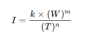
Where:
I is maximum current;
W is trace width;
T is trace thickness; and
K, m, and n are the constants.
PCB Trace Resistance Calculator
We don’t think that we need to explain what the PCB trace resistance calculator does, but just in case, it calculates the resistance of traces in PCBs. There are multiple online calculators but you can do it manually by using the given formula.
R = ρL/TW (1+α(Tamb−25°C)
Where:
L is the length of the trace;
T is the thickness of the trace;
W is the width of the trace;
R is the resistance; and Tamb is the ambient temperature.
PCB Trace Impedance Calculator
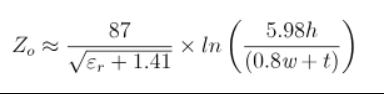
Where:
-
Z₀ = Characteristic impedance of the trace (in ohms)
-
εᵣ = Relative permittivity (dielectric constant) of the PCB material
-
h = Height from the trace to the reference plane (in mils)
-
w = Width of the trace (in mils)
-
t = Thickness of the trace (in mils)
The PCB trace impedance calculator will help make the initial design easy as it will allow the user to input basic parameters and get a calculated impedance according to the IPC-2141 standard. There are multiple online calculators accessible but you can also use the following formula to calculate the impedance.
PCB Trace Repair

You should also acquire knowledge on how to repair PCB trace issues as it's equally important. If your power supply unit exhibits problems such as unusual noise or display failure then it needs PCB trace repair. Also, make sure that you have a PCB trace repair kit. As mentioned below is a guide on all steps of PCB trace repair:
· In the first step, locate the damaged trace on the PCB.
· Carefully remove the damaged trace by using a cutting tool. And, also take care that you do not harm the nearby components in any way.
· Clean the damaged area until it displays a copper color and apply solder to the exposed regions.
· Use a solvent-cleaning pen or a cleaning paper towel to clean the repair area to get rid of debris. After doing that, apply flux to the existing track and use a soldering iron to help in soldering both sections of the track.
· Make a selection of suitable replacement wire that is in good condition and of the appropriate size.
· Tin the ends of the replacement wire.
· If your chosen replacement wire is suitable, then remove the insulation from both ends and solder it in place.
· In the next step, solder one end of the replacement wire. To add more, make sure that a section of the new wire overlaps the existing trace by at least twice the width of the PCB trace. Secure the wire with the tape and then apply flux to the overlap. Now solder the wire and trace it together.
· Now, shape the wire flexibly according to requirements and specific needs.
· Make sure to attach the wire securely to the surface of the circuit board using adhesive or tape.
· Finally, solder the other end of the replacement wire.
· After soldering, complete the repair process and make sure the connection is normal. Clean any remaining stains or residue.
Conclusion
To sum up, designing a PCB trace takes attention and planning to detail and even small mistakes can cause big problems. As you know every project is different, so what is ideal for one project may not work appropriately for another. Therefore, think about your particular needs such as whether are you designing for high-speed data. Or handling large currents? Then choose a trace design based on the purpose of the circuit.
PCBasic will assist you if you need further help with anything. Let our experts help you create optimized PCB traces that ensure optimal functioning. Contact us now and let us assist you with bringing the PCB design to reality!
 About PCBasic
Time is money in your projects – and PCBasic gets it. PCBasic is a PCB assembly company that delivers fast, flawless results every time. Our comprehensive PCB assembly services include expert engineering support at every step, ensuring top quality in every board. As a leading PCB assembly manufacturer, we provide a one-stop solution that streamlines your supply chain. Partner with our advanced PCB prototype factory for quick turnarounds and superior results you can trust.