Global high-mix volume high-speed PCBA manufacturer
9:00 -18:00, Mon. - Fri. (GMT+8)
9:00 -12:00, Sat. (GMT+8)
(Except Chinese public holidays)
Global high-mix volume high-speed PCBA manufacturer
9:00 -18:00, Mon. - Fri. (GMT+8)
9:00 -12:00, Sat. (GMT+8)
(Except Chinese public holidays)
HomePage > Blog > Knowledge Base > PCB Stackup: A Comprehensive Guide
The PCB of most devices that works reliably at very high speeds and accuracy is usually designed to have several layers that manage the power distribution and high-speed signal routes. NVIDIA's GeForce RTX 30-series GPUs have boards with about 20 layers to manage the different graphics card functionality. Does that mean the higher the number of layers, the better the board is?
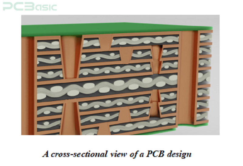
In recent times, various industries, such as consumer electronics, telecommunication, and more, have adopted the use of multilayer PCB (PCB stackup), mainly to eradicate noise, create a more sophisticated version of their product, and also improve the overall efficiency of a PCB, In 2023 multilayer PCB market worth approximately 88.1 billion US Dollars. It’s projected to grow to closely 145.09 billion dollars by 2032. In a nutshell, any PCB designer who will remain relevant must have mastered PCB stackup best practices. The expansion we see in the 5G technology and electric vehicles will require more sophisticated multilayer boards in the future.
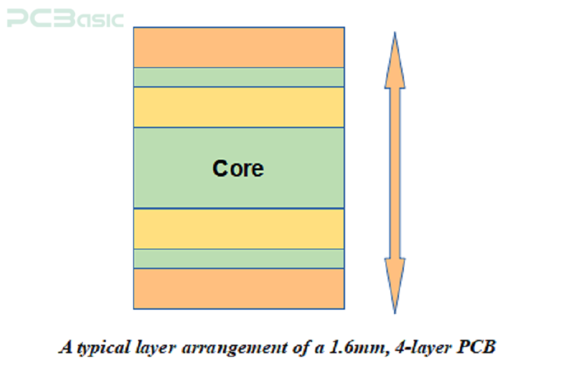
PCB stackup refers to the arrangement of each layer in a printed circuit board, mainly focusing on the electrical properties of each layer and the entire board. In PCB design, much attention is paid to the stackup because it's the primary determinant of the board's vulnerability to external noise, crosstalk, and electromagnetic interference. It is safe to infer that the overall efficiency of any PCB depends not only on the circuit's correctness; wrong circuit stacking can equally mess up a perfectly designed circuitry.
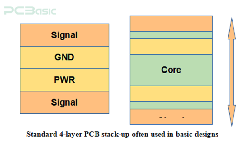
The image below perfectly represents a PCB layer stackup. There, we have a graphical representation of a 4-layer PCB with an assumed thickness of 1.6 mm. Each layer focuses on a different electrical signal. Layers 1 and 4 are the signal plane, while layer 2 is the ground plane (GND), and layer 3 is the power plane (PWR).
It is true that stacking up at times makes the PCB manufacturing and assembly process more complex, affecting the cost and ease of manufacturing and assembly. Why do PCB designers still stack different layers in a PCB design when a circuit design can be easily represented on a one—or two-sided board? To answer this accurately, we’ll have to look into the effect of a well-thought-out PCB stackup in a PCB design.
Signal Integrity Management: In a typical circuit where signals (especially high-frequency and RF signals ) are being transferred from one part of the board to another, the circuit is mainly vulnerable to signal reflection, loss, and crosstalk if not correctly managed. PCB Stackup gives the designer more flexibility and control to prevent or greatly reduce these potential issues when implemented carefully. Careful implementation in this context includes the strategic arrangement of each layer and control of the trace impedance among the circuit traces.
Electromagnetic Interference (EMI) Control: EMI occurs when the electromagnetic field generated in a circuit interferes with another circuit, causing noise or other issues in the circuit. One common way EMI is managed in a circuit is by placing ground layers adjacent to a signal layer. This implies that a coordinated PCB stackup is essential for EMI eradication.
Thermal management: Of what use is a that heats up uncontrollably powered? Thermal management is crucial in designing a reliable PCB. In most high-power and high-speed circuits with excessive heat, you can significantly improve heat dissipation by carefully planning your stackup. Selecting the right materials (such as copper for efficient thermal conductivity), the thickness of a layer, and the calculated use of the ground plane helps with the proper dispersion of heat across a board.
PCB stackup can be categorized into different types, mainly depending on the application and design requirements. Each design uniquely affects the PCB’s performance, flexibility, heat dissipation, and several other features. Here are four common PCB types you must know as a PCB designer or aspiring PCB designer.
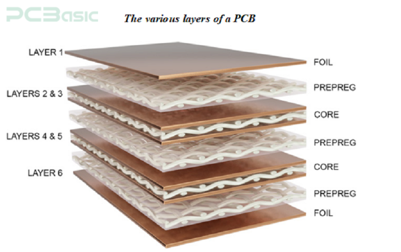
Multilayer PCB Stackup: Multilayer PCBs have at least three layers of conductive materials separated by dielectric (insulating) layers. The inner signal, power, or ground are sandwiched between the dielectric materials, and the overall number of layers ranges from 4 to above 30. However, the design gets complex with an increased number of layers.
Many advanced electronics boards, including computer motherboards, smartphone boards, medical devices, and many more, are multilayer stack-ups. Their ability to handle interference and crosstalk makes them ideal for high-speed designs such as SMPS (Switch Mode Power Supply). The complexity is worth their ability to handle interference and crosstalk.
HDI (High-Density Interconnect) PCB Stackup: You can quickly identify an HDI PCB stackup by its extra-tiny, close layers. It has an increased wire density and uses micro-vias with an aspect ratio of 0.751, blind and buried vias, and fine and super-tiny traces.
Whenever you think of miniaturization, think of HDI PCB stackup. They’re mainly used when there’s a space constraint or high-speed requirements. You will find them in smartphones, wearables, and other compact electronics. HDI PCB stackup are built using sequential lamination.
Flex and Rigid-Flex PCB Stackup: Flexible PCB stack-up are made from flexible materials (such as polyimide), making them bendable without breaking. In like manner, rigid-flex PCB stackup have a combination of layers made with flexible and rigid materials, and they are carefully designed to handle stresses when bent.
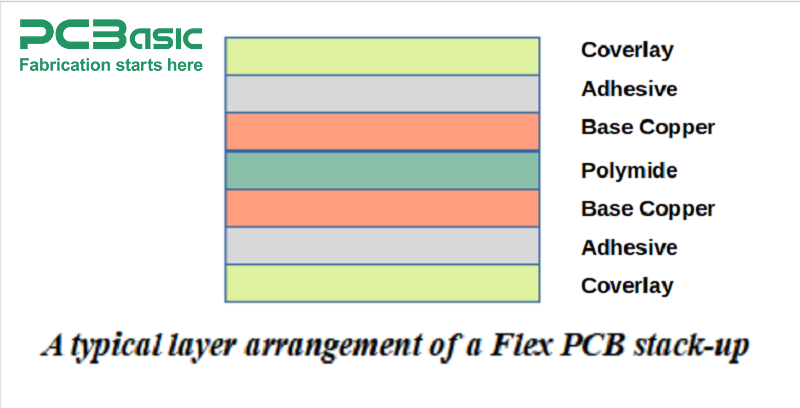
They fit well into unique shapes and can handle movement without breaking. They are found in medical devices, aerospace, and other applications that require adaptability to movement and vibration.
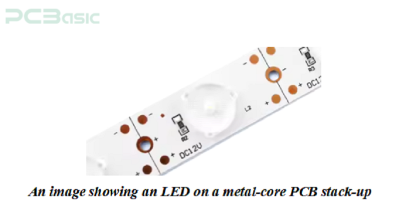
Metal Core PCB Stack-Up: You may have seen one of these boards in LED lighting. Metal core PCBs have metal layers, usually aluminum or copper, and they are highly suitable for excess heat dissipation. MCPCBs generally eradicate the need for an extra heat sink and prevent components from getting damaged due to heat. They are commonly used in LED lighting and other high-power applications.
PCB stackup is supposed to achieve some goals in PCB design, and these goals must be clearly defined and understood before you start the design. Understanding your design goals and requirements will guide you in deciding the perfect number of layers to use, the thickness of each layer, the material selection for each stack, and other technical considerations required.
While focusing on the outcome of the design, you must understand the manufacturer's capability and tailor your design to pass the DFM (Design for manufacturer's) check. The systematic approach employed while deciding the best PCB stackup types and properties to implement for a design must include at least putting all of the following into consideration:
· EMC/EMI Performance: Electromagnetic Compatability and Electromagnetic interference must be a significant part of the consideration in PCB stackup [elimination of EMI won’t happen by haphazard arrangement of layers. Intentional effort must be made to pair a power plane with a ground plane to suppress the radiation of electromagnetic waves and ground planes must be placed adjacent to signal planes to shield the remaining part of the circuit from noise.
· Power Distribution: When planning your PCB design the understanding of the circuit's power distribution will greatly affect your your stackup plan. Proper planning will prevent the circuit from unnecessarily heating up, causing voltage drop and losses across the circuit.
· Signal Integrity: The purpose of the PCB stackup is defeated if the signal traveling across the circuit experiences distortion, crosstalk, or delay. In high-frequency applications, high-frequency signals are often isolated and sandwiched between ground layers to shield them from interference. It takes intentional and careful planning of each layer arrangement to achieve good signal integrity.
The overall properties of your board, which include the layer count, spacing, and material choice for the PCB stack-up, are primarily the determinants of the PCB’s efficiency and functionality. Your design should focus on getting an optimized board with minimal issues.
You can decide what layer comes first, follows, and last in your PCB design, and your design will still pass the DFM check. With several options to choose from, you need to decide which is best for your design. Here are a few tips that will guide your PCB stack-up choice.
· To manage Signal Integrity and EMI in your design, you have to understand that energy flows in the dielectric space between the copper layer and the conductor plate, which is just a waveguide. Close coupling of the signal and ground layer, as well as the power and ground layer, will prevent the field from spreading.
· The coupling of two signal planes together will cause crosstalk in the circuit.
· Decreasing the distance between the Power and Ground planes increases the capacitance in your PCB and reduces the inductance. Hence, choosing the right dielectric material and decreasing the layer thickness can reduce EMI in a PCB design.
· Striplines (i.e., a signal or power plane sandwiched between a ground plane) are best for containing fields in higher-energy or higher-speed signals.
It's important to ensure that your design goals, approach, and layout are within the confines of the manufacturer's capabilities. If, for instance, you are manufacturing your PCB with Company XXX, you must check their requirements and adjust your design to what is manufacturable. Software such as Altium Designer, KiCad, and Eagle allow users to configure the DRC setting according to the manufacturer's requirements. If a PCB manufacturer can produce a maximum of 16 layers PCB stackup, you must ensure your design doesn't exceed the requirement.
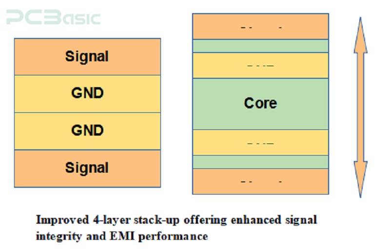
To better understand the different techniques used in PCB stack-up, let’s consider two variations of the 4-layer PCB stack-up. One is the [Signal, Prepreg, GND, Core, PWR, Prepreg, Signal+PWR], a typical configuration many consider a standard. The other is [Signal+PWR, Prepreg, GND, Core, GND, Prepreg, Signal+PWR], which is believed to be a better configuration.
The first configuration has the top signal layer and power plane paired with the ground plane, which is perfect for ensuring good signal integrity. However, the down signal layer is still directly adjacent to the power layer, making the system susceptible to noise. This justifies why it’s not considered a great option.
The second configuration has the power and signal strategically routed on the same plane, which is still okay. Both signal and power planes are paired with a ground plane, which will ensure good signal integrity and reduce EMI in the board.
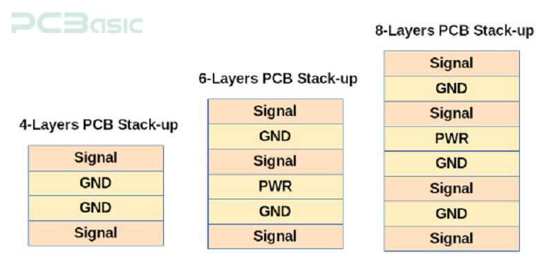
There are several examples of PCB stackup from different numbers of layers to different arrangements; they include:
· 4-layer PCB stackup
· 6-layer PCB stackup
· 8-layer PCB stackup
If you have followed this article this far, you should know that the PCB stackup is not only for professionals to showcase their design skills but also for everyone who wishes to design boards with higher efficiency and better performance. Each of the planes in the stack must be strategically placed to either solve the EMI problem, optimize signal integrity, or ensure the system's overall efficiency. There's no point in having a complex and expensive design infested with crosstalk.
Take into consideration every tip and piece of information in this article when designing your next board, and in no time, you'll have mastered the art of designing PCBs with greater accuracy.

Assembly Enquiry
Instant Quote
Phone contact

+86-755-27218592
In addition, we've prepared a Help Center. We recommend checking it before reaching out, as your question and its answer may already be clearly explained there.
Wechat Support

In addition, we've prepared a Help Center. We recommend checking it before reaching out, as your question and its answer may already be clearly explained there.
WhatsApp Support

In addition, we've prepared a Help Center. We recommend checking it before reaching out, as your question and its answer may already be clearly explained there.