Global high-mix volume high-speed PCBA manufacturer
9:00 -18:00, Mon. - Fri. (GMT+8)
9:00 -12:00, Sat. (GMT+8)
(Except Chinese public holidays)
Global high-mix volume high-speed PCBA manufacturer
9:00 -18:00, Mon. - Fri. (GMT+8)
9:00 -12:00, Sat. (GMT+8)
(Except Chinese public holidays)
HomePage > Blog > Knowledge Base > PCB Milling | A Comprehensive Guide
Do you know PCB milling? Whether you know it or not, read this article first. After reading it, you will definitely gain something.

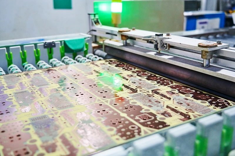
PCB milling is a common and widely used process in electronic manufacturing, which is used to process precise circuit patterns on substrates. Compared with traditional chemical etching (PCB Etching), it does not rely on chemical solvents and etching liquids but removes materials through mechanical processing to form the required circuit pattern. This method can not only significantly improve the efficiency of circuit board production but also effectively save costs and reduce material waste, which also makes it one of the ideal choices in modern electronic manufacturing. The following is a comprehensive introduction to the PCB milling process, including definition, process flow, equipment and tools, as well as its advantages and specific applications in manufacturing.
PCB milling is a precise and efficient circuit board manufacturing process. In the PCB milling process, CNC equipment is used. This equipment will physically mill the PCB board mechanically according to the designed pattern to remove unnecessary materials, thereby forming precise circuit patterns and connections. The copper layer is removed by controlling the movement of the cutter to form the required conductive path in the milling process, so the control of the tool movement must be precise. In addition, PCB milling is particularly suitable for manufacturing environments with high environmental requirements because it does not rely on chemical solvents, and can also be flexibly used in small-batch production and prototype development, which makes this technology increasingly popular.

Unlike traditional chemical etching, PCB milling is a mechanical process where the milling cutter moves along the path defined in the PCB design file to remove material only in the required areas. This process has high requirements for processing accuracy and plate quality, so it requires precise parameter settings.
The success of PCB milling depends largely on its design parameters. Please see some key design parameters listed below:
1. Board quality
Carefully consider the hardness and thickness of the board, because the choice of material will affect the quality of milling (for example, thicker copper foil requires different milling speeds and feed rates, otherwise it may cause severe tool wear). If you want a material with good stability and durability, I recommend FR4 and other common composite materials (PCBasic will provide the best choice based on your needs). Also, consider the flatness of the board surface because this is very important for the "precise control of the tool" mentioned earlier.
2. Milling parameters
Milling parameters include tool diameter, cutting depth, feed rate and speed, cutting path, etc. The setting of these parameters plays a very critical role in PCB milling. If the set parameters are not suitable for the PCB to be produced, it will definitely produce undesirable results. For example, for harder materials or thicker copper layers, I set the feed rate and speed very high, then after a while, the tool must have severe wear and the cut pattern is not clear. The solution is to use lower feed rate and speed for hard materials or thicker copper layers, and higher speed for softer materials. So, set the appropriate milling parameters for milling PCB.
3. PCB Milling Methods
|
Process Method |
Description |
Applicable Scenarios |
|
Laser Milling |
Using high energy density laser beams to precisely remove material |
High-precision and intricate circuit pattern machining |
|
CNC Router Milling |
Typically used for cutting PCB outlines and forming slots |
Mass production and outline cutting |
|
Carbide End Mills |
Effectively cuts copper foil without damaging the substrate, typically used for detailed copper foil cutting or small structure machining |
Small-batch production, detailed copper cutting, and small structure machining |
|
Plated Slots |
Creates plated slots on PCBs to connect multiple layers and enhance conductivity |
Multi-layer boards and applications requiring electrical connections |
4. Design for Manufacturing Manual for Milling
DFM guides manufacturers on how to optimize the design to reduce errors and costs in actual production, which is the key to successfully milling PCB.
|
Feature |
PCB Milling |
PCB Etching |
|
Environmental Impact |
High, no chemical waste |
Low, produces chemical waste |
|
Precision |
High |
Moderate |
|
Processing Time |
Short |
Longer |
|
Cost |
Moderate to High |
Lower |
|
Suitable for |
Small batches, complex designs |
Large-scale production |
The high manufacturing precision of PCB milling can ensure the quality of each PCB, and compared with etching, it produces less waste and does not involve chemicals. In addition, PCB milling is fast and efficient, which greatly shortens the product development cycle. It is more suitable for prototype design and small batch production that require high precision, and it can help companies bring them to market faster.
PCB milling is also widely used. Its high reliability and low failure rate make it particularly suitable for prototype design, military electronics, automotive electronics and other fields.
|
Problems |
Causes |
Solutions |
|
Edge Whitening |
During PCB milling, if the milling force exceeds the bonding strength of the substrate, localized delamination occurs between resin and fiberglass, causing edge whitening. |
① Adjust the milling force and use appropriate milling parameters and tools. ② Use high-quality substrates. |
|
Tool Wear
|
One of the most common issues; Poor quality of tool material; high-quality machining requirements from the customer; |
① Use higher hardness tool materials (e.g., carbide tools). ② Optimize the machining process to reduce tool wear. ③ Regularly maintain and replace worn tools in a timely manner. |
|
Low Machining Accuracy |
Incorrect machining process; improper milling parameter settings. |
① Optimize the machining process, and set appropriate feed rate, rotation speed, and cutting depth parameters. ② Ensure the tool moves as perpendicularly as possible. ③ Use high-precision machines and tools for machining. |
|
High Milling Temperature |
Friction between the tool and workpiece easily raises cutting temperature, which reduces cutting efficiency and shortens tool life. |
① Use cooling systems, such as coolant sprayers, to reduce tool surface temperature promptly. ② Choose appropriate tool materials and coatings. |
|
Static Electricity |
Friction during the milling process generates static electricity. |
① Use anti-static devices or measures during milling, such as humidifiers or ion blowers. ② Use anti-static workbenches and fixture materials. ③ Maintain appropriate humidity levels in the processing environment. |

Assembly Enquiry
Instant Quote
Phone contact

+86-755-27218592
In addition, we've prepared a Help Center. We recommend checking it before reaching out, as your question and its answer may already be clearly explained there.
Wechat Support

In addition, we've prepared a Help Center. We recommend checking it before reaching out, as your question and its answer may already be clearly explained there.
WhatsApp Support

In addition, we've prepared a Help Center. We recommend checking it before reaching out, as your question and its answer may already be clearly explained there.