Global high-mix volume high-speed PCBA manufacturer
9:00 -18:00, Mon. - Fri. (GMT+8)
9:00 -12:00, Sat. (GMT+8)
(Except Chinese public holidays)
Global high-mix volume high-speed PCBA manufacturer
9:00 -18:00, Mon. - Fri. (GMT+8)
9:00 -12:00, Sat. (GMT+8)
(Except Chinese public holidays)
HomePage > Blog > Knowledge Base > A Comprehensive Guide to PCB Design and Assembly
In PCB design, you need to develop circuit schematic diagrams and PCB layout diagrams. This PCB design includes the placement positions of components and the electric path routing. Meanwhile, in PCB assembly, PCB manufacturers will install electronic components according to the PCB design. These components include capacitors, resistors and integrated circuits.
Understanding what a PCB is, how to design a PCB and what PCB assembly is can help ensure
accurate printed circuit board assembly. The role of a PCB designer is to ensure that the PCB design and layout are suitable for reliable PCB assembly services and to take into account what materials the circuit board is composed of.
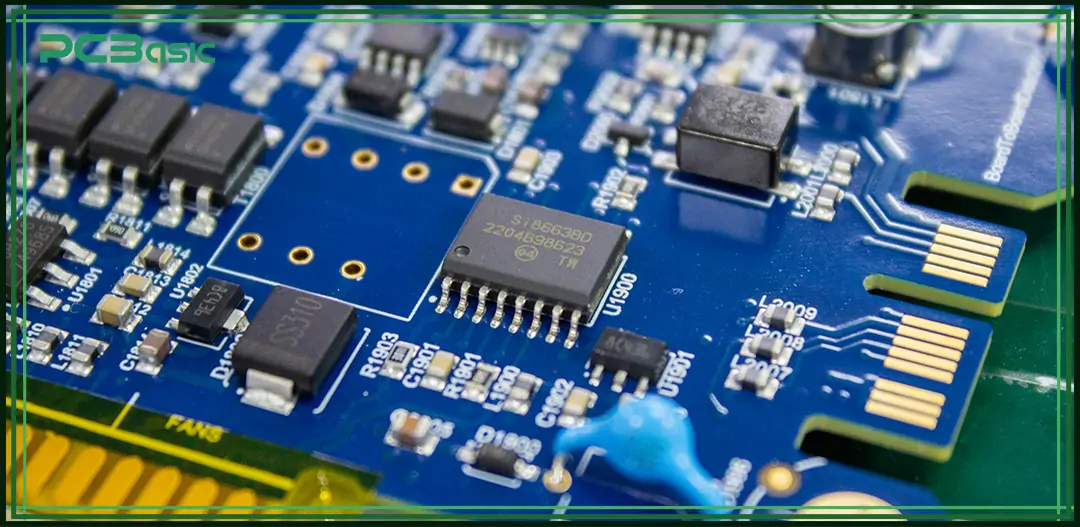
Let's start with the basics: What is a PCB? The Printed circuit board (PCB) is a flat board that achieves mechanical support and electrical connection of electronic components through conductive circuits, pads and other structures etched from copper foil.
These circuit boards are the core of modern electronic products. Understanding what a PCB is assembly helps engineers develop various products ranging from wearable devices to industrial controllers.
A printed circuit board is not a single plate. It has numerous layers. Interestingly, each layer is developed to deliver a specific function. You will read the details below.
The substrate is the basic substrate. What is its function? It makes the conductive layers stable. Subsequently, it fights against heat, strain, and electrical loads.
FR4 is a pretty popular epoxy. In contemporary gadgets, water-repellant features have become crucial. Therefore, contemporary PCB manufacturers prefer to work with FR4 materials.
Polyimide material makes the PCB base flexible. So it helps the PCB to flex and be compliant with surfaces. This material offers low electronic noise and perform under high temperatures.
They arrange conductive pathways on PCB surfaces. Because this material contains great electrical properties, it does not let the PCB parts, like communication systems and RF, hold excessive heat.
Metal core substrates are usually made with aluminum or copper. They tackle problematic heat generation. That is the must-have feature for applications like power equipment and LEDs.
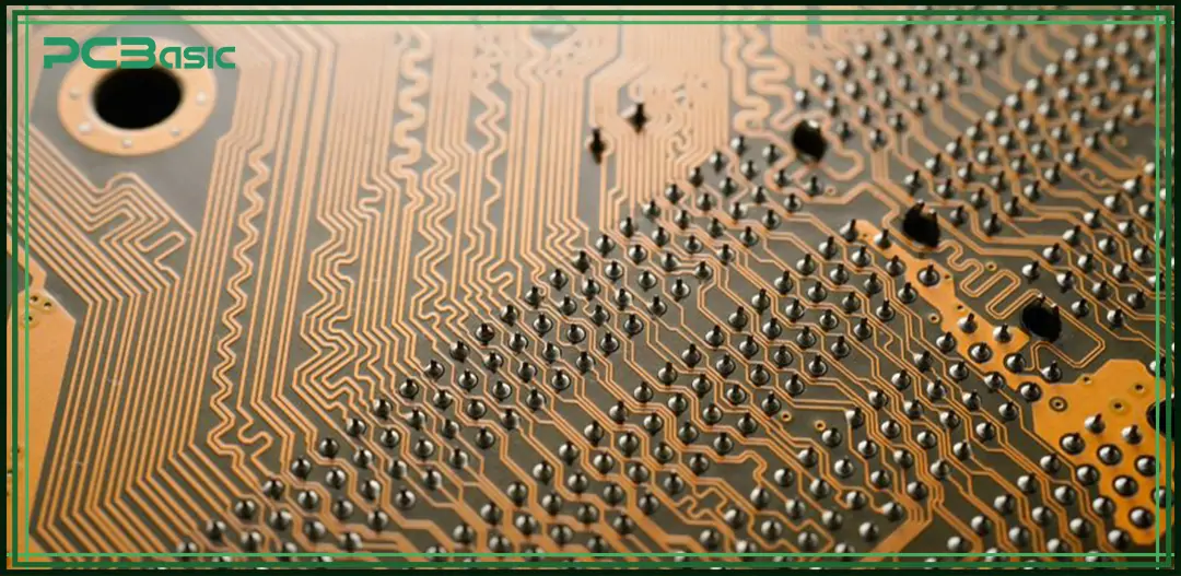
The electric routes that connect components are made of layers of copper. These are the layers used for the transmission of signals and power on the PCB.
Conductivity: Copper, being a highly conductive metal, allows for better signal and power transmission.
Copper thickness: The copper thickness affects the amount of current that the PCB will carry.
1 oz/ft² indicates the weight of copper spread over one square foot, corresponding to a thickness of approximately 35 microns.
It is a thicker film for the conduction of large currents. You can find this material in power supplies and motor controllers.
Between the copper-made layers is a layer of dielectric, an insulating material. This prevents short circuits from occurring, ensuring the PCB will operate correctly.
Dielectric Constant
The dielectric constant measures the storage capacity of a material's electrical energy. Higher DK sees how much material absorbs electrical charge compared to a vacuum. Lower ones are suitable for parts enabling larger signal speeds. Like microwave transmission lines, RF, and digital circuits.
It indicates the propagation of signal power. That is absorbed by the material as thermal energy. Depending on its structure and glass resin induction, Df is good for high-frequency assemblies.
• Epoxy Resin
• PTFE (Polytetrafluoroethylene)
• Dielectric Ceramic
Solder masks are a thin lacquer. It is made of polymer. This layer protects the copper traces. In many cases, there always remains a chance for oxidation.
Reduces Bridges: Stops solder from flowing in the wrong direction
Copper Protection: Prevents oxidation and corrosion.
Easier to View: Copper traces and pads are more visible.
Silkscreen—the uppermost layer printed on the solder mask. It provides labels and hints to aid in assembling and organizing the problems.
Component Labeling: Labels parts, pins and directions
Assembly Guidance: Assists in placing components, whether manually or through automation.
Testing Aid: Marks the testing points and critical connections for testing purposes.
A specialized use case for PCBs requires advanced PCB materials because there are additional demands to be met.
Where to start for making PCB assemblies? It involves the same few steps. But precision, creativity, and technical capability are paramount. That will cater to each stage, like well-working, productive, and budget.
• Identify the Design Needs
• Routing
• Power and Ground Planes
• Simulation and Verification
• Design Rule Checks
• File Generation
Take the first step by making a functionality list of PCBs. That is subject to a particular product weighing environmental conditions. Mention the required size, detailed dimension, necessity of layers, and component placements.
PCB designers create the visual design of a PCB. Why do they make it? The reason is to show how components will be interconnected. Moreover, it will be easy to detect errors. Therefore, it is recommended to focus on precise documentation.
It represents the wider continuous areas. That is focused on distributing the power supply voltage and electric signals. The noise in the signals can often be minimized by separation.
Use specialized software to build a virtual model. In this way, you can analyze the signal reflections, electronic behavior, thermal hotspots, or crosstalk issues.
Automated checks ensure your layout is compliant with the manufacturable tolerances such as minimum trace width, distance between traces (spacing), and via size.
Exporting files such as Gerber and drill files, and other manufacturing documents. You should check these diligently to ensure they match what you are designing.
 About PCBasic
Time is money in your projects – and PCBasic gets it. PCBasic is a PCB assembly company that delivers fast, flawless results every time. Our comprehensive PCB assembly services include expert engineering support at every step, ensuring top quality in every board. As a leading PCB assembly manufacturer, we provide a one-stop solution that streamlines your supply chain. Partner with our advanced PCB prototype factory for quick turnarounds and superior results you can trust.
PCB assembly (PCBA) converts an ordinary PCB to a complete electronic circuit by mounting and soldering components. This means that there is technology and concrete measures that allow every part to do its own job efficiently.
There are the main types of PCB assembly methods:
Components are attached to the PCB surface. Surface Mount Technology (SMT) aids in more components per unit area and is thus well suited for modern miniaturized devices.
To solder components with leads, you should insert them in pre-drilled holes. For the mechanical strength, connector components are removed from THT.
Integrates SMT and THT to benefit from the best of both worlds.
You have made a PCB design and manufactured it so what is next? The next step is assembly. PCB manufacturers install small parts all over the board. Let’s read the different steps involved in PCBA.
PCB manufacturers can apply solder paste on the board, which provides temporary adhesion for parts.
A stainless-steel stencil with holes is placed over the PCB. Solder paste—a mix of flux and solder powder—is applied over the stencil with a squeegee. That paste only sticks where pads are exposed. Components will be laid on top of it.
Components are placed on the PCB in areas where voids of solder paste have already been applied. This step can be done machine or handwork based on design.
Machines that get products from one point in a factory to another automatically are called automated pick-and-place machines. Components are placed with pinpoint accuracy by miniaturized high-speed machines.
These machines read the design file to know where each component goes. Parts are taken from reels or trays and placed directly onto the solder paste.
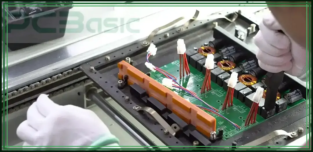
Suitable for one-off, bigger, and lower volume designs. Operators manually place large components, for example, connectors or transformers.
Reflow soldering, used for surface mount technology (SMT) components This allows solder paste to liquefy and later harden. It creates electrical connections that are not only very long-lasting but also possess mechanical strength.
The solder paste PCB was placed on the belt running into a reflow oven. The board goes through the following stepwise heating in an oven:
Preheating: Start with slow heating to ensure thermal shock is avoided.
Soak: Holds the temperature steady to obtain flux activation from the solder paste.
Reflow: Rises to a temperature that liquifies the solder (~250°C for lead-free solder)
Cooling: Slowly reduce the temperature to freeze the solder.
For through-hole (THT) components, we use wave soldering. This is most effective when you have leads of parts that go into holes in the PCB.
Held at an angle, the PCB is tracked across a stream of molten solder. Solder applies to the exposed leads, and it fills the holes so there are strong connections.
PCB assembly companies incorporate IPA into clean-soldered components. It helps significantly to clear flux residue and dust from the board.
Cameras scan the board for wrongly installed components. AOI also identifies poor solder joints, such as insufficient solder, bridging, etc.
Apply to invisible solder joints like in Ball Grid Array (BGA) parts. In-situ detection of voids, cracks, or insufficient solder below the component.
Functional testing is important to check the entire assembly instead of the components. At this step, the power sources are applied to run the device.
It is the final stage to examine. That, whether the parts are working properly or not under simulated real-time practice.
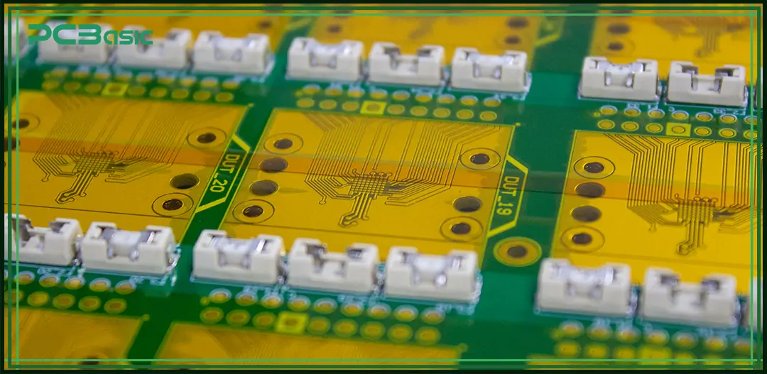
You would be an expert in PCB design basics and assembly. However, here, you will read some very useful tips to improve your design and assembly.
The first stage is Design:
1. Precise schematic is something you must be very careful about. It is recommended to incorporate visible symbols and labels.
2. The second tip is to double check your layout. Why this is important because it will reduce your crosstalk and signal length.
3. The best tip is to incorporate DRC so you can identify the issues on time.
2nd Stage is Assembly:
1. Always go to a reliable supplier because they can supply you with top-rated parts.
2. Simultaneously, choose reflow or wave soldering to make very powerful joints.
3. Never forget to run an inspection test. It will help you to identify any missing components.
When it comes to dependable PCB manufacturing and printed circuit board assembly, PCBasic stands out as a trusted partner. We deliver high-quality solutions tailored for a wide range of industries, ensuring every board meets your expectations in performance and reliability.
Full-Service Support from PCB Design to Production
With over 10 years of PCB design experience and project management know-how, PCBasic offers end-to-end services—from schematic creation and PCB layout to fabrication and PCB assembly. Our experienced PCB designers ensure your project runs smoothly from concept to final product.
Dual-Factory System for Any Batch Size
PCBasic operates two specialized facilities:
• Shenzhen focuses on fast-turn, small-batch PCB assembly services
• Huizhou handles high-volume PCB manufacturing with streamlined production lines
This structure enables us to support startups, engineers, and large enterprises with equal efficiency.
Scalable, Smart, and Precise PCB Assembly Services
We use advanced equipment and processes to handle complex PCB assembly needs. Whether it’s surface mount, through-hole, or mixed technology, our precision-driven approach ensures high-quality PCB assemblies at every stage.
Why Choose PCBasic?
• Complete control of what a PCB is and how to design a PCB
• Deep understanding of what circuit boards are made of for material optimization
• In-house stencil and fixture production for rapid turnaround
• Intelligent warehouse for stable component supply
PCBasic is your go-to provider for reliable, efficient, and scalable PCB design and PCB assembly services.
Before coming to a conclusion, you must have understood the fundamentals of PCB design and assembly. You have read the steps above for designing a PCB and core substrate materials. Moreover, how can you make PCB assembly successful?
If you need a PCB with an impeccable design, manufacturing, and assembly, contact PCBasic. Our company incorporates an instant quoting engine for PCB manufacturing and assembly orders.
Assembly Enquiry
Instant Quote
Phone contact

+86-755-27218592
In addition, we've prepared a Help Center. We recommend checking it before reaching out, as your question and its answer may already be clearly explained there.
Wechat Support

In addition, we've prepared a Help Center. We recommend checking it before reaching out, as your question and its answer may already be clearly explained there.
WhatsApp Support

In addition, we've prepared a Help Center. We recommend checking it before reaching out, as your question and its answer may already be clearly explained there.