Global high-mix volume high-speed PCBA manufacturer
9:00 -18:00, Mon. - Fri. (GMT+8)
9:00 -12:00, Sat. (GMT+8)
(Except Chinese public holidays)
Global high-mix volume high-speed PCBA manufacturer
9:00 -18:00, Mon. - Fri. (GMT+8)
9:00 -12:00, Sat. (GMT+8)
(Except Chinese public holidays)
HomePage > Blog > Knowledge Base > Aspect Ratio in PCB industry
The aspect ratio is a factor that proves very crucial in PCB fabrication, via plating, and reliability during board use. The PCB aspect ratio is defined as the ratio of the PCB thickness to the drilled hole diameter. The aspect ratio greatly affects how printed circuit boards are manufactured and their performance.
A high aspect ratio in PCB design can lead to difficulties in via plating, causing inconsistencies in copper deposition and reducing the board's durability. This is especially important for the micro via aspect ratio in HDI (High-Density Interconnect) PCBs, where the hole sizes are significantly smaller.
Knowing the PCB aspect ratio provides designers and manufacturers with the essential guidance for choosing the correct PCB hole size and proper standard drill sizes for PCB design to improve production and electrical integrity.

For PCBs, the aspect ratio is defined as the thickness of a PCB to the diameter of the drilled hole. It is a key factor in drilling and PCB manufacturing, affecting design feasibility, reliability, and production yield.
The aspect ratio in PCB is defined as:
Aspect Ratio = PCB Thickness / Drilled Hole Diameter

For instance, in a PCB with a thickness of 1.6 mm and a drilled hole of 0.2mm diameter, the aspect ratio would be 8:1.
1. Drilling Constraints: A high via aspect ratio complicates drilling, especially microvia aspect ratios for HDI boards (High-Density Interconnects).
2. Plating Uniformity: High aspect ratios can cause uneven copper plating in the hole walls, affecting conductivity and reliability.
3. Manufacturing Limits: Most manufacturers follow PCB-standard drill sizes that limit aspect ratios to guarantee production assurance and yield.
The PCB aspect ratio is determined using a concise formula based on comparing the thickness of the PCB to the diameter of the drilled hole.
Aspect Ratio = PCB Thickness / Drilled Hole Diameter
This calculation is essential to determine manufacturability, especially concerning PCB drilling and via aspect ratio limitations.
Let’s suppose we have a PCB with the following specs:
● PCB Thickness: 1.6 mm
● Drilled Hole Diameter: 0.4 mm
Using the formula:
Aspect Ratio = 1.6 mm / 0.4 mm = 4:1
This means the hole depth is four times the diameter of the hole.
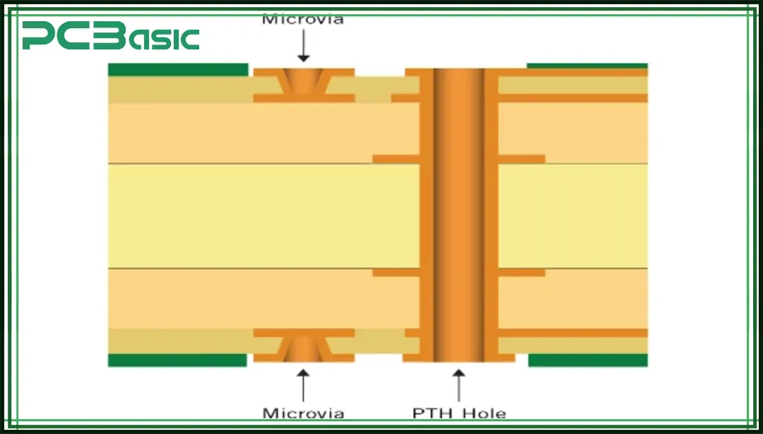
● Through-Hole Vias: They usually have an aspect ratio of about 6:1 to 10:1. The ratio will depend on the standard PCB drill sizes and associated plating processes.
● Microvia Aspect Ratio: Microvias that are used in HDI PCBs have a very low aspect ratio, normally ≤ 1:1; these are laser-drilled and do not go through the entire thickness of the PCB.
● Higher aspect ratios (greater than 10:1) bring about inconsistencies in plating, resulting in weak connections.
● The fabrication processes to maintain more accuracy of PCB hole size will be required for the smaller drilled holes.
● Balanced aspect ratios tend to raise the yield and reliability during manufacturing while reducing the possibility of open circuits and plating failures.
By proper aspect ratio calculation in PCB design, certain performance impacts can be optimized, but manufacturability must also be assured within the limits of the industry.

The aspect ratio is not fixed and varies depending on manufacturing capabilities, hole sizes, and standard drill sizes. Here is a reference table with typical PCB aspect ratios based on industry standards:
|
PCB Thickness (mm) |
Minimum Drilled Hole Diameter (mm) |
Aspect Ratio |
|
0.8 |
0.2 |
4:1 |
|
1.0 |
0.2 |
5:1 |
|
1.2 |
0.25 |
4.8:1 |
|
1.6 |
0.3 |
5.3:1 |
|
2.0 |
0.35 |
5.7:1 |
|
2.4 |
0.4 |
6:1 |
|
3.2 |
0.5 |
6.4:1 |
Microvia Aspect Ratio Guidelines
For the microvia aspect ratios, they can go in very low values because they are laser-drilled.
Microvia
Depth (mm)
Microvia
Diameter (mm)
Aspect
Ratio
0.1
0.1
1:1
0.15
0.125
1.2:1
0.2
0.15
1.3:1
● High aspect ratios (over 10:1) can lead to difficulties in drilling and plating PCBs.
● Standard PCB through-hole vias should have an aspect ratio ≤ 10:1 for proper copper plating.
● Microvias must have an aspect ratio of 1:1 or lower to ensure reliability in HDI PCB designs.
● This varies according to PCB manufacturers; therefore, it is prudent to check with them before approving the design.
Guided by these PCB aspect ratio specifications, manufacturability can be achieved, defects reduced, and PCB performance optimized.
PCB aspect ratio forms a critical consideration in PCB design and manufacturing, which directly influences the feasibility of PCB drilling, via plating, and reliability overall. By knowing the relationship between PCB thickness and PCB hole size, engineers can further optimize designs with met standards that promote high-quality production.
For through-hole vias, the aspect ratio between PCB should be maintained below 10:1 to avoid any plating issues, while microvia aspect ratio should be ≤ 1:1 for reliability enhancement in HDI designs.
Following the standard manual and recommendations from PCB manufacturers for PCB standard drill sizes would ensure good manufacturability and a minimum defect rate.
Understanding this design aspect encourages optimality in the finished PCB performance, enhanced lifespan, and cost-effectiveness. Whether for standard or high-density interconnect (HDI) applications, keeping aspect ratio under control is essential for the success of a PCB.

Assembly Enquiry
Instant Quote
Phone contact

+86-755-27218592
In addition, we've prepared a Help Center. We recommend checking it before reaching out, as your question and its answer may already be clearly explained there.
Wechat Support

In addition, we've prepared a Help Center. We recommend checking it before reaching out, as your question and its answer may already be clearly explained there.
WhatsApp Support

In addition, we've prepared a Help Center. We recommend checking it before reaching out, as your question and its answer may already be clearly explained there.