Printed circuit boards (PCBs) are integral components of modern electronics. PCBs provide the foundation to mount and connect electronic parts from cell phones to appliances.
While early PCBs used just one copper layer, advances in manufacturing now enable PCBs with multiple layers.
This article explores the different types of PCB layers, when to use them, and the advantages of single, double, and multilayer boards. Understanding PCB layers helps create efficient printed circuit board designs tailored to any application.
So, let's get right into the article without wasting more time.
What is a PCB Layer?
A PCB layer is each thin sheet of conductive copper incorporated into the circuit board. While the simplest PCBs have just two layers (top and bottom layers), additional layers can be inserted in between as needed.
Every layer serves a distinct purpose, providing pathways to route electrical connections between components. The number of layers impacts the complexity and cost of fabricating a PCB.
More layers allow greater flexibility in laying out a schematic but increase expenses for materials and production. Optimizing the layer count provides sufficient wiring space without over-engineering the design.
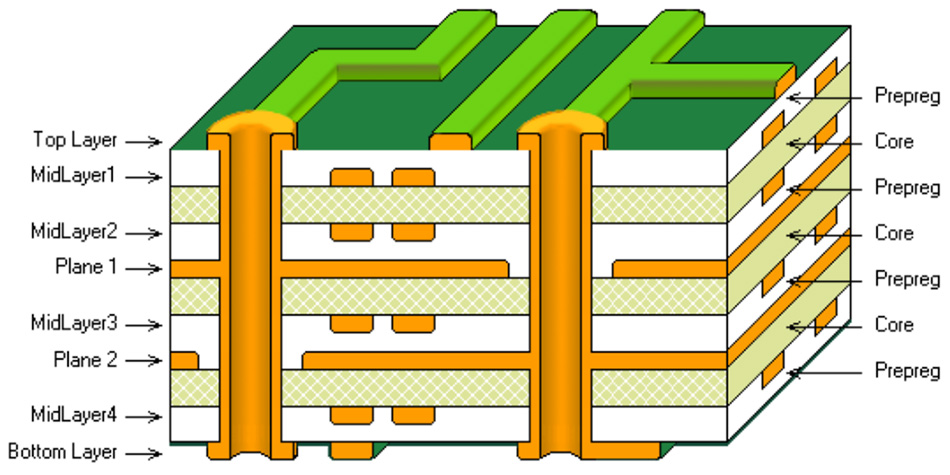
A sheet of insulating dielectric material separates each conductive layer. Common dielectrics include FR-4 fiberglass, polyimide, and ceramic substrates. Vias consisting of plated through holes connect traces between layers as required.
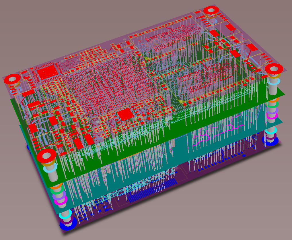
Careful stacking of copper and dielectric builds up a multilayer board able to incorporate thousands of traces in a compact area.
What is a Single Layer PCB?
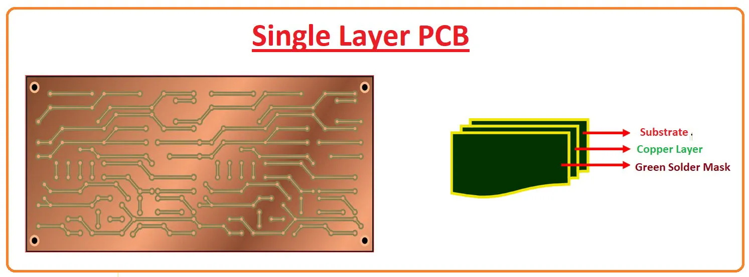
A single-layer PCB contains just one layer of conductive copper traces on a non-conductive insulating substrate. Components mounted on one side, their leads soldered to the exposed traces. The other side may feature graphical silkscreen markings for identification.
Single-layer PCBs emerged early in the development of printed circuit technology. They offered a low-cost method to connect components using etched copper traces instead of hand-wired points-to-point connections.
While limited in routing capacity, single-layer PCBs adequately support simple, low-density circuits. Manufacturing only requires a single etching process and drill operation, keeping fabrication straightforward and economical.

Advantages of Single-Layer Board Design
The innate simplicity of a single-layer board imparts some natural benefits:
● Low production costs due to minimal material and process requirements
● Quick fabrication turnaround times
● Straightforward circuit layout without complex multilayer constraints
● Adequate for applications with minimal trace routing needs
● Facilitates high-volume manufacturing and rapid assembly
● Repairs are generally easy by accessing all conductors from one side
Limitations of Single-Layer PCB:
● Single-layer PCB capabilities lag behind multilayer counterparts
● Restricted surface area limits component density
● Lack of ground and power planes may compromise signal integrity
● High-speed signals require impedance control through layer stacking
● Adds size and weight when expanded functionality requires larger boards
Typical Applications of Single-Layer PCB
Despite inherent limitations, single-layer PCBs still provide the ideal balance of simplicity and capability for:
● Basic consumer electronics like coffee makers and clock radios
● Low-frequency analog sensor and actuator circuits
● LED lighting drivers
● Power supply regulators
● Educational trainers and DIY hobby boards
So, while multilayer PCBs dominate complex electronics, tried and true single-layer boards continue serving many cost-sensitive and low-density applications.
What are Multilayer PCBs?
As electronic devices become more complex, the demands on PCBs increase accordingly. This has led to the proliferation of multilayer PCBs, which offer enhanced capacity and routing flexibility compared to simple single or double-layer boards.
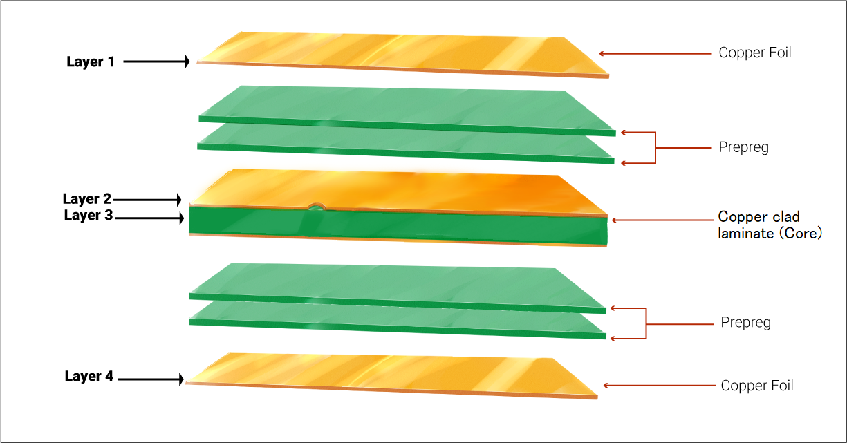
Constructing a multilayer PCB entails laminating alternating layers of insulating and conductive materials using high heat and pressure. The insulating dielectric layers, typically fiberglass-reinforced epoxy, separate the conductive copper layers and prevent electrical shorts.
Sophisticated ceramic or fluoropolymer dielectrics enable multilayer PCBs to operate at higher frequencies and temperatures. The lamination process ensures uniform bonding between layers without voids that could undermine performance and reliability.
Multilayer PCBs comprise the backbone of countless high-tech systems, including computers, telecommunications infrastructure, medical diagnostic equipment, and aerospace avionics.
Their expanded real estate and routing density readily accommodate the elaborate circuitry of these devices. For example, the multilayer PCB within a smartphone may contain over a dozen layers to integrate the various subsystems and components.
Advantages of Multilayer PCBs
The foremost advantage of multilayer PCBs is their ability to integrate complex, dense circuitry within a compact footprint. Each layer provides additional surface area for tracing conductors and placing components.
This facilitates minimizing the overall size of the PCB while meeting the interconnect requirements. Multilayer construction enhances mechanical ruggedness and stability, as the laminated dielectric materials inhibit twisting or warping.
Limitations of Multilayer PCBs
However, multilayer PCBs carry higher costs compared to simpler versions. The lamination process demands additional materials, equipment, and expertise, translating to higher fabrication expenses.
Repairing faults within internal layers poses difficulties as well. Hence, engineers must evaluate the benefits and tradeoffs when selecting multilayer PCBs for an application.
Rigorous design practices and testing help ensure the finished boards operate reliably over their target service lifetimes.
So, where does this lead?
Continued advancements in materials, fabrication methods, and design tools empower electrical engineers to push the envelope with multilayer PCB capabilities. This propels the development of smaller, faster, and more powerful electronic devices that shape technological progress. Mastering multilayer PCB intricacies remains an essential competency for PCB designers and engineers.
2 Layer PCB: Economy and Simplicity

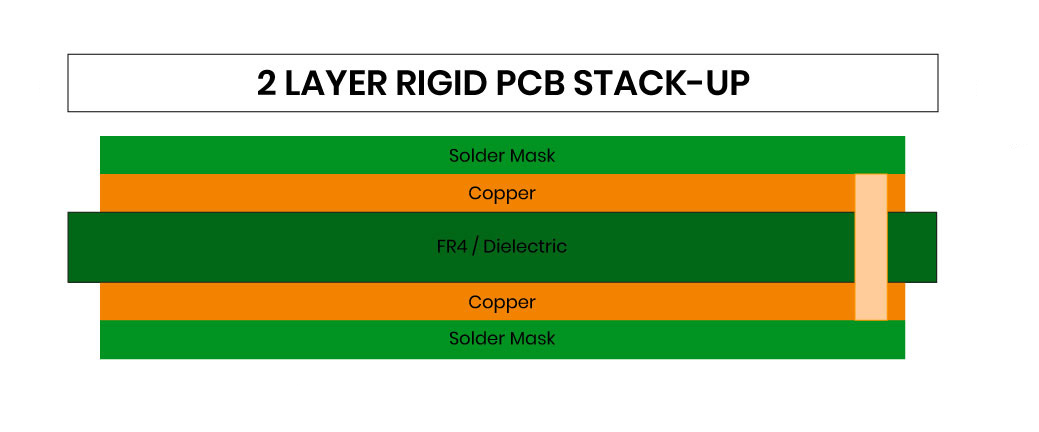
The two-layer or double-sided PCB offers the most affordable option, sandwiching a single insulating core between thin copper layers on either side. Components mount on both exterior surfaces, enabling moderate density.
However, the limited board real estate strains the intricate routing of dense or high-speed circuits. Vias puncture the core to interconnect the top and bottom layers but consume space themselves.
Two-layer boards work well for cost-sensitive, low-complexity applications. The simple construction also facilitates assembly and repair.
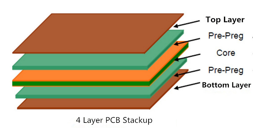
4 Layer PCB: Enhanced Capability

Two additional inner copper planes flank a thicker insulating core in four-layer PCBs, typically serving as power distribution and ground reference layers. Segregating power and ground enhances signal integrity and reduces noise.
The extra routing space eases trace layout and enables higher component density versus two-layer versions. Four-layer stack-ups also improve mechanical stability and thermal dissipation.
The board can be configured with more signal layers by assigning multiple functions across the four layers. The moderately increased fabrication complexity is warranted for many applications requiring more excellent capability than simple two-layer boards can provide.
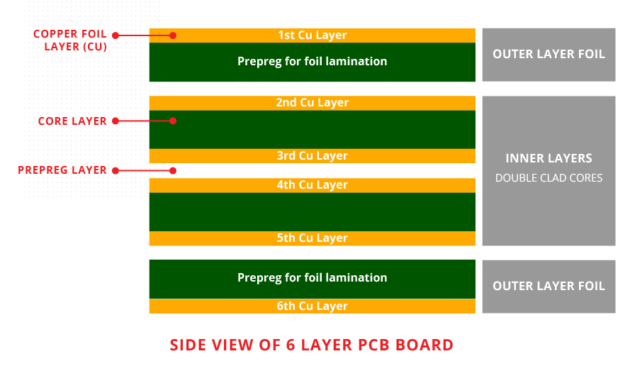
6 Layer PCB: Balancing Signals and Shielding

In six-layer PCBs, two additional inner layers augment the four-layer stack up. Typically configured as a signal-power-ground-signal-power-signal arrangement, this stack balances traces and shielding.
The two internal ground and power planes isolate the middle signal layers from each other and external interference. This enables denser, higher-speed routing than four-layer versions can support.
The outer layers handle lower-speed traces and component placements. So, the six-layer stackup furnishes sufficient signaling and shielding for many complex designs.
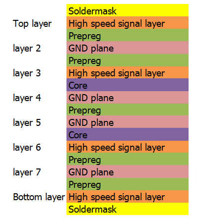
8 Layer PCB: Connecting High-Density Circuits

For even greater demands, eight-layer PCBs incorporate two more signal layers. The stackup often utilizes multiple ground plane layers to enhance shielding and isolation between signals.
This facilitates routing high-density circuits with fast edge rates and stringent signal integrity requirements. The additional layers also allow thicker, lower impedance power distribution traces to furnish robust current to components without voltage drops.
In short, the expanded capacity of eight-layer PCBs makes them ideal for high-speed, high-complexity systems where performance is paramount.
How to Carefully Select the Appropriate PCB Layer Stackups
When planning PCB layer stackups, engineers weigh factors such as signal integrity, power delivery, thermal dissipation, manufacturability, and cost. The optimal choice depends on circuit complexity and routing density.
Simulation and modeling tools help optimize stack-up configurations. While PCB boards with more layers have many advantages, two-layer versions offer easier repair and remain the most cost-effective option when design simplicity permits.
The tradeoffs between capability and fabrication costs incentivize utilizing the minimum number of layers that satisfy the design goals. So, understanding this helps engineers to match designs to the appropriate stack up.
Types of PCB Layers
Printed circuit boards (PCBs) contain a stack of conductive copper and insulating dielectric layers to route traces and isolate signals. Here are some of the core PCB layer types and their roles in the design:

Mechanical Layers
The primary mechanical layer precisely defines the physical boundaries and dimensions of the PCB for fabrication and assembly purposes. It outlines the board's length, width, shape, and corner radii.
Additional auxiliary mechanical layers can specify details like physical cutouts, tabs, tooling holes, edges, and other non-conductive mechanical elements. However, most PCB designs only require a single mechanical layer.
Keep-Out Layers
Keep-out layers help constrain the layout by delineating exclusion zones where components or routing cannot be placed. For example, keep-outs may reserve space around the board perimeter or internal areas that must remain clear of parts and traces for assembly or service access.
Keep-outs act as visual aids during routing and enable rapid checking for violations. They help optimize component spacing and trace routing density.
Signal Routing Layers
The top, bottom, and internal signal layers contain the copper traces that interconnect electronic components. Surface mount and through-hole parts are attached to pads on the outer layers.
Traces route signals between pads, vias, and components placed across the PCB. Careful trace routing strives to achieve impedance matching, minimize crosstalk, control EMI, and meet circuit timing requirements. High-density designs may require multiple signal routing layers both internally and on the outer surfaces.
Power and Ground Planes
Entire layers dedicated as low-impedance reference planes distribute power and ground voltages uniformly across the PCB area. This provides clean, steady voltage supplies to components and enables robust return paths.
Planes also serve as low-impedance AC references, improving signal integrity compared to discrete traces. Large areas of contiguous copper effectively dissipate heat as well. Decoupling capacitors placed near IC loads helps further reduce noise on the power distribution.
Split Power and Ground Planes
Split planes allow the segmentation of power and ground layers into isolated regions containing different voltages. For example, a split ground plane can provide analog and digital ground zones to prevent noise coupling.
Split power planes may supply multiple voltage levels required by various components. Careful placement of segmentation lines and component assignments is needed to utilize split planes effectively.
Solder Mask Layers
A solder mask is a coat of insulating lacquer or other protective polymer selectively applied to the PCB surface. It prevents oxidation and electrical shorting from contaminants like debris or condensation.
However, it leaves crucial areas uncovered, like component pads and vias, to allow soldering. The solder mask visually delineates the conduction and isolation areas. Minimum web widths must be maintained between mask openings to prevent voltage breakdown.
Solder Paste Layers
Solder paste layers indicate the pads and areas that require solder paste application before surface mount components are placed. The paste improves capillary flow between leads and pads during reflow soldering.
Proper paste deposition facilitates assembly and optimizes solder joint quality. Solder paste layers are generally required for designs utilizing fine-pitch packaged parts.
Silkscreen Layers
Silkscreen printing applies component identifiers, reference designators, board titles, markings, and other printable text to the surface finish. This aids in visual inspection, manufacturing, troubleshooting, inventory tracking, and service of PCB assemblies.
Silkscreens typically use the solder mask layer as a background. Allowances must be made for registration tolerances between the mask and silkscreen. Silkscreens are usually confined to the exterior layers only.
FAQs About PCB Layers
1). Is It Possible to Have a 7-layer PCB?
Yes, 7-layer PCBs are undoubtedly feasible. Odd layer counts allow symmetric stack-ups with a central core and equal layer divisions on either side. This provides good signal isolation and heat dissipation. The additional layers furnish more routing flexibility compared to 6-layer boards.
2). How Do You Determine the Number of Layers in a PCB?
The number of layers depends on the circuit complexity, routing density, component count, and performance requirements. More layers allow increased trace routing space and segregation of critical signals. High-speed designs may need more layers to maintain signal integrity.
3). How Thick is a PCB Layer?
The standard PCB layer thickness is 1-ounce copper, equivalent to around 1.4 mils (35 microns). Thicker 2-ounce copper further enhances conductivity and heat dissipation. Dielectric core thickness in multilayer boards typically ranges from 2 to 8 mils depending on the number of layers.
4). What's the Maximum Layer of a PCB?
There is no specific maximum number of layers in multilayer PCB fabrication. Complex designs like high-end FPGAs and networking chips may incorporate 20 layers or more. However, extremely high layer counts impose fabrication challenges and expenses. Most commercial PCBs for cost-sensitive consumer applications are at most 12 layers.
Conclusion
In summary, printed circuit board layers enable the routing density and signal isolation vital for sophisticated electronics. Single-layer PCB boards suffice for basic, low-cost designs, while multilayer boards support complex functionality.
Two-, four-, six-, and eight-layer stack-ups offer incremental enhancements as more layers allow increased routing capacity and segregation of signals. Careful layer configuration also facilitates impedance control and power delivery.
While adding layers increases fabrication complexity, the expanded capabilities often warrant the tradeoff for high-density circuits. Matching the layer count to the design constraints helps balance performance, cost, and manufacturability when planning PCB stackups.
