Global high-mix volume high-speed PCBA manufacturer
9:00 -18:00, Mon. - Fri. (GMT+8)
9:00 -12:00, Sat. (GMT+8)
(Except Chinese public holidays)
Global high-mix volume high-speed PCBA manufacturer
9:00 -18:00, Mon. - Fri. (GMT+8)
9:00 -12:00, Sat. (GMT+8)
(Except Chinese public holidays)
HomePage > Blog > Knowledge Base > IC Package Technology:A Comprehensive Guide
In this comprehensive guide, we will explore the different IC packaging types, their characteristics, and the rules to follow when designing and selecting the right IC package.
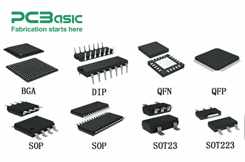
An IC package is a physical enclosure that contains an integrated circuit (IC) and provides the electrical connections. This packaging serves the dual purpose of protecting the IC and of assisting thermal dissipation thereby facilitating proper electrical connections to the chips and electronic devices.
There are numerous IC package types available in the market, each optimized for a different purpose and for different performance needs. Below are examples of common IC package types used in modern devices.
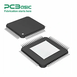
SMD (Surface Mount Device) package is a widely used type of IC package which can be directly soldered to the surface of the PCB (printed circuit board) without mounting holes. SMD package is very compact in size and can be used in low-profile designs. Such packages can support a wide range of integrated circuits and handle heat dissipation efficiently.
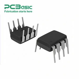
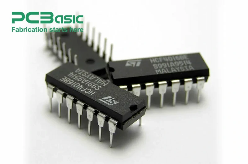
The DIP package is one of the oldest IC package types and it is still commonly used today. The DIP IC package provides two rows of pins in parallel, making it easy to insert them into the PCB through-hole. Although DIP packages are bigger than SMD packages, they are still used in applications where assembly and repairs can be done manually, typically for low-frequency and low-profile circuits.
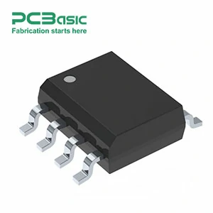
The SOIC package is an SMD package that has a smaller and thinner construction than the DIP package. The SOIC package is one of the most common IC packaging styles utilized in modern electronics from communications equipment to automotive applications because of the compact size and heat dissipation efficiency. The SOIC meaning refers to its small outline design, which is low-profile whereby it is a better solution for electronic devices.
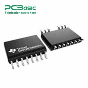
SOP packages are similar to SOIC packages but with typically more pins than an SOIC packages, so they are suited for ICs with higher pin counts. SOP packages, also surface mount types, are made to be compatible with automated assembly processes like SMT assembly. SOP packages are widely adopted for different electronic devices to strike a good compromise between small size and pin density.
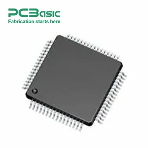
The QFP is a flat package having pins on four sides of the package. The QFP IC packing style is frequently used in even higher performance applications as it allows for even more pins. These packages come in several different sizes for versatile applications. QFP packages are designed for high-frequency circuits and ideal for applications that require strong electrical connections.
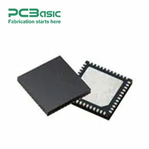
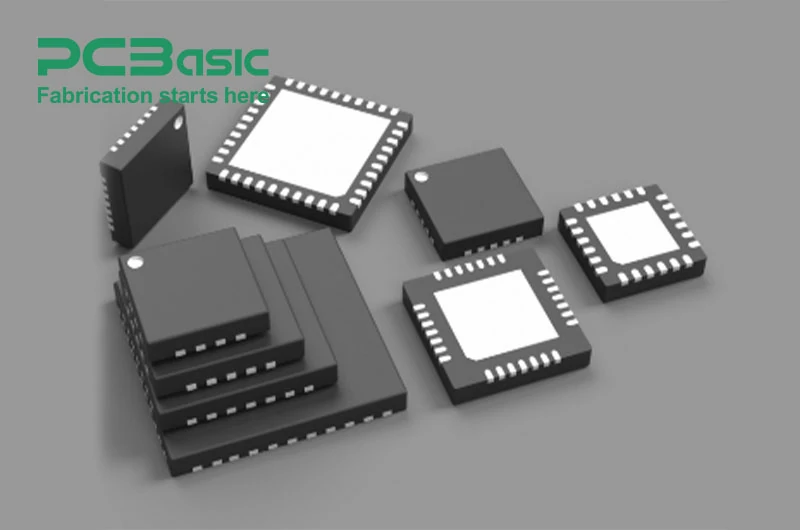
The QFN package is basically a QFP package, but it does not have any pins around the package. The pads are not conventional pads, but rather QFN IC package-style pads and they are oriented at the bottom of the package for surface mount. This package is especially ideal for low-profile designs and is widely used in high-speed, high-heat applications.
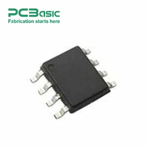
SOT packages are mainly applied to transistors, but other types of integrated circuits can be also packaged in this package. It is a low-profile, compact SMD package for space-limited applications. SOT packages are commonly employed on low-frequency, low-power circuits and can be mounted using surface mount technology (SMT).
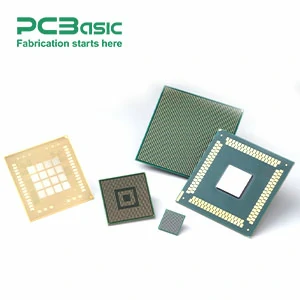
The Ball grid Array (BGA) is a relatively new type of IC package type for high-performance applications. The BGA IC package style features a grid of balls, or bumps, soldered to the bottom side of the package. This package offers both good heat dissipation and is capable for high-speed electrical connections. BGA is widely adopted for high-frequency and high-density circuits like graphics processor and microprocessor for advanced electronic devices.
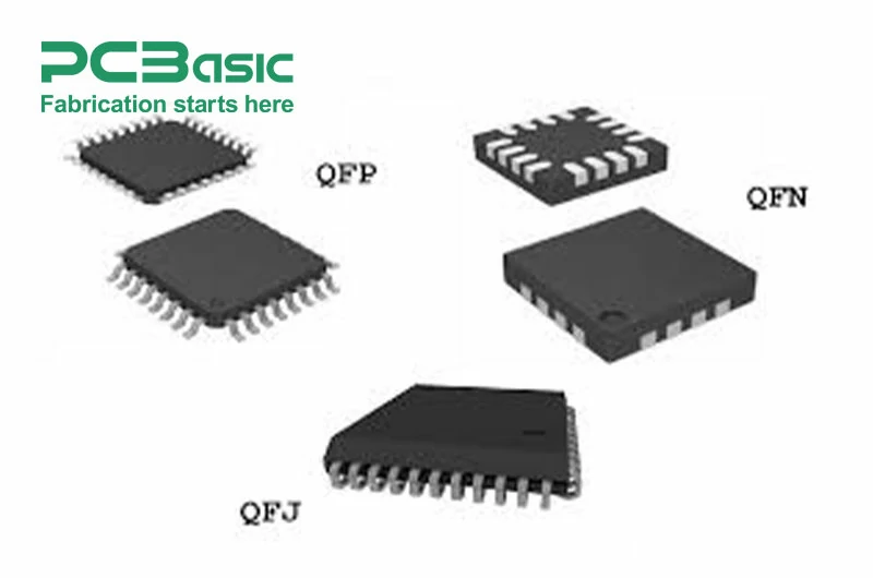
A typical IC package (Integrated Circuit Package) includes the following components and details.
Core Functionality: The central component of the package, contains the actual electronic circuitry.
Wafer Layers: The chip is manufactured from a series of microfabricated wafers containing transistors, capacitors, resistors, and other components.
Protection Purpose: The primary goal of packaging is to protect the IC chip from mechanical damage, moisture, dust, and other external factors.
Electrical Connection Method: This refers to the interface between the IC package and the printed circuit board (PCB), typically in the form of pins or pads.
Number and Arrangement of Pins:
DIP (Dual Inline Package): Dual rows of straight pins.
QFP (Quad Flat Package): Flat leads on all four sides.
BGA (Ball Grid Array): Solder balls arranged in a grid underneath the package.
Function Assignment: Each pin or pad serves a specific function, such as power supply, ground, input/output signals, or control signals, typically detailed in the datasheet.
External Dimensions:
Includes length, width, and height, usually measured in millimeters or inches.
Pitch and Layout:
Pin pitch refers to the distance between the centers of adjacent pins, which is critical for PCB design.
Pad layout specifies the shape and position of solder pads for proper alignment.
Compatibility: The size of the package determines if it fits the PCB design.
Heat Management: IC chips generate heat during operation, and the package design must include thermal management solutions to maintain performance and reliability.
Thermal Solutions:
Heatsinks: Metal fins or conductive materials to dissipate heat from the chip's surface.
Thermal Pads: Some packages have dedicated thermal pads at the bottom to enhance heat dissipation.
Thermal Resistance: Packaging specifications often include thermal resistance values (e.g., θJA and θJC), indicating the efficiency of heat transfer from the chip to its environment.
Identification Information:
Printed information on the package surface, including IC model number, lot number, production date, and manufacturer logo, facilitates identification and traceability.
Standard Compliance: Packages may include symbols indicating compliance with standards like RoHS (Restriction of Hazardous Substances).
Anti-Counterfeiting Marks: High-end ICs may feature security marks, such as laser etching or QR codes, to verify authenticity.
Orientation Marks: For example, BGA packages often have dots or notches to indicate the correct installation orientation.
Material Composition: Packages are often made of plastic, ceramic, or metal, each with different mechanical strength and thermal expansion properties.
Durability: The mechanical design ensures the chip can withstand vibration, shock, and prolonged operating conditions.
Sealing: Certain packages, such as ceramic ones, provide higher hermeticity, making them suitable for high-reliability applications in aerospace and military sectors.
There are many rules for IC package design so that package should be compatible on the PCB layer and get the least short between electrical connections and have excellent mechanical reasons. These include — but are not limited to — the following key considerations:
Compatibility with PCB layout: Ensure that the package size matches the available space on the PCB and that the pin arrangement is aligned with the design.
Heat dissipation: Consider heat dissipation requirements and choose a package with an appropriate thermal management solution.
Pin density: Select an IC package type that can accommodate the required number of pins.
Package size: Choose a package that balances cost-effectiveness and performance. Smaller packages like QFN and BGA cost more but offer better performance in high-speed applications.
Reliability: Consider factors such as mechanical stress, vibration and temperature fluctuations, which may affect the performance of the package.
Choosing the right IC package requires understanding the requirements of the application, including performance, size, and budget. Here are a few tips for choosing the right IC package:
1. Performance requirements: For high-speed or high-frequency applications, consider BGA, QFP or QFN packages, which provide better electrical connection and heat dissipation performance.
2. Size limitations: For low-height designs, SMD packages (such as SOIC or SOP) are ideal for minimizing space requirements.
3. Assembly method: If SMT assembly is required, SMD packages compatible with automated processes, such as SOIC, QFP and BGA, can be selected.
4. Cost considerations: For designs with limited budgets, DIP and SOP packages may provide a more cost-effective solution without sacrificing essential functionality.
Finally, IC packaging is one of the essential components of modern electronics that affects the performance cost and reliability of electronic devices. IC package types range from SMD packages to BGA IC package style, each offering advantages for specific applications and many more that you might consider as well.
Knowing the various choices available, such as SOIC IC package style, QFP IC package, and QFN, will help designers choose the IC package that fits their purposes. In the end, picking the right IC packaging means preserving the performance and the lifetime of the integrated circuits behind the most critical technologies in our lives.

Assembly Enquiry
Instant Quote
Phone contact

+86-755-27218592
In addition, we've prepared a Help Center. We recommend checking it before reaching out, as your question and its answer may already be clearly explained there.
Wechat Support

In addition, we've prepared a Help Center. We recommend checking it before reaching out, as your question and its answer may already be clearly explained there.
WhatsApp Support

In addition, we've prepared a Help Center. We recommend checking it before reaching out, as your question and its answer may already be clearly explained there.