Do you know that your printed circuit board works better and lasts longer when you get the copper thickness right? The wrong thickness choice might risk your project malfunctioning because of inadequate current power flow. So what exactly does 1 oz copper thickness mean for this purpose? It's a must-go term for engineers, designers, and manufacturers because it affects how well your PCB handles power, dissipates heat, and runs efficiently. To select an appropriate copper thickness for your project, start by learning about 1 oz copper thickness through this explanation covering its definition, measurement methods, and important selection criteria. No matter whether you're new to PCB design or want to learn better, go through the sections below to get the gist of 1 oz copper thickness.

What is 1 oz Copper?
As the name tells us, 1 oz. copper thickness means spreading a thin layer of copper material across one square foot. If we do the mathematics here, 1 oz copper thickness equals 35 microns and converts to both 0.035 millimeters and 1.4 mils.
Now that you know the conversions and basics, you might be wondering who uses standard 1 oz copper board. Usually, it is used as a top layer for the base material, such as FR4. Why? Because it gives sufficient conductivity to your circuit for low-to-medium current transmission without excessive loads of resistance.
Moreover, using 1 oz. copper thickness gives you the advantage of transferring electrical current across your device without heating up and raising any additional internal temperatures. Generally, a 1 mm copper trace plated at 1 oz copper thickness can support at least 4 amps of electrical flow with a slight temperature increase of just 10 degrees C.
How Thick is 1 oz Copper?
In terms of mathematics, 1 oz copper is basically 0.035 mm. If you’re wondering how is this so, then here’s a simple breakdown for you.
1 oz/ft² means 1 ounce of copper covers one square foot of area.
To calculate the thickness:
● The density of copper is 8.96 g/cm³.
● 1 ounce (oz) = 28.3495 grams.
● 1 square foot = 929.03 cm².
● Using the formula for thickness:
Now, let’s plug in the values:
Besides the 1 oz thickness, you can also see other variations. For instance, widely used copper thicknesses are:
● 1 oz Copper = 0.035 mm (35 µm)
● 2 oz Copper = 0.070 mm (70 µm)
● 3 oz Copper = 0.105 mm (105 µm)
To simplify things for you, here’s a copper thickness chart explaining different copper thicknesses and their conversions into millimeters, micrometers, and mills.
|
Copper Weight (oz/ft²)
|
Thickness (mm)
|
Thickness (µm)
|
Thickness (mils)
|
|
0.5 oz
|
0.0175 mm
|
17.5 µm
|
0.7 mils
|
|
1 oz
|
0.035 mm
|
35 µm
|
1.37 mils
|
|
2 oz
|
0.070 mm
|
70 µm
|
2.74 mils
|
|
3 oz
|
0.105 mm
|
105 µm
|
4.11 mils
|
|
4 oz
|
0.140 mm
|
140 µm
|
5.48 mils
|
|
5 oz
|
0.175 mm
|
175 µm
|
6.85 mils
|
Key Properties of 1 oz Copper
1 oz copper in printed circuit boards (PCBs) provides a balance of thickness and conductivity suitable for most standard applications. Let's have a look at some key properties of 1 oz copper.
1. Electrical Conductivity
Circuit designs benefit strongly from 1 oz copper because it transports electricity exceptionally well. For instance, the 1 oz copper provides reliable electrical flow across PCB traces to handle up to 20 amps, which ensures your design functions correctly. In this regard, three main factors determine how well it functions. What are they?
1. Its current carrying capacity
2. Trace width
3. The amount of resistance and temperature shifts
2. Thermal Conductivity
Another important property of 1 oz copper is its very pliable, that is having perfect thermal conductivity. PCBs do make good use with them for dissipating heat and keeping the thermal stability balanced in heavy operational conditions. There is just enough heat dissipation at 1 oz thickness to keep the PCBs from thermal overload, and the PCB levels keep these components within non-destructive temperature limits.
3. Mechanical Robustness
Our main criterion when selecting the right PCB thickness is its mechanical stability performance. By selecting 1 oz copper you gain peace of mind because it strengthens circuit performance while ensuring mechanical strength for durable designs. The material keeps its flexible properties along with a reliable ability to stand up against physical force. Moreover, with 1 oz copper-thick boards, your devices can withstand a great amount of corrosion and rust. However, you must apply solder masks and electroless plating for additional protection.
4. Cost-Effectiveness and Versatility
From a financial point of view, 1 oz. copper is a cheap alternative for PCB manufacturing. Its performance is great and affordable. Moreover, it is often a standard pick for most industrial uses. 1 oz. copper is such an all-rounder that it can be used for signal transmission, power delivery and grounding systems that solve the various needs PCB designers have in all industries.
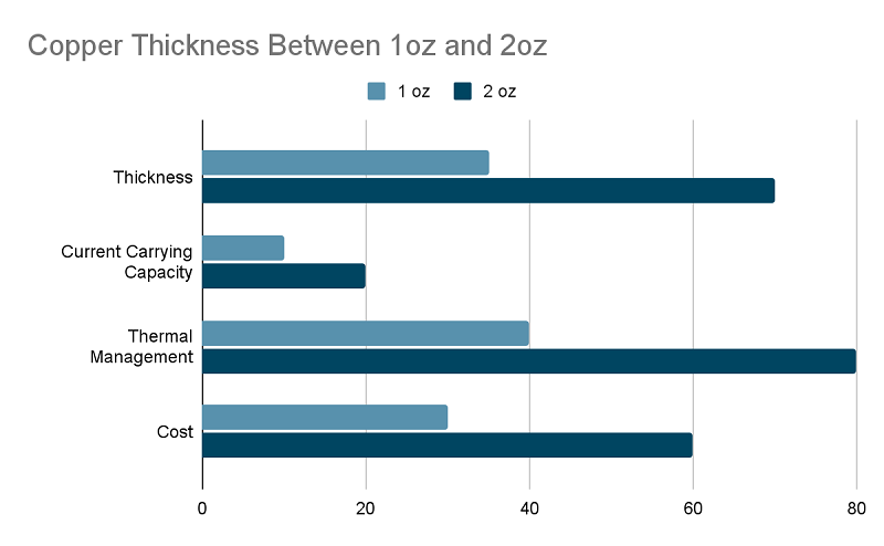
1 oz Copper vs. Other Copper Weights
Let’s now compare different copper weight along with their currency carrying capacity and uses.
|
Aspect
|
1 oz Copper
|
2 oz Copper
|
|
Thickness
|
35 µm (0.035 mm)
|
70 µm (0.070 mm)
|
|
Current Carrying Capacity
|
They are used for moderate applications. Suitable for most low to medium-power circuits.
|
High; ideal for circuits requiring greater current.
|
|
Thermal Management
|
Standard heat dissipation; sufficient for general use.
|
Superior heat dissipation; prevents overheating.
|
|
Cost
|
Economical; widely used in standard applications.
|
Higher cost due to increased material usage.
|
|
Usage
|
Consumer electronics, general-purpose PCBs.
|
Power supplies, industrial equipment, and automotive electronics
|
PCB Design Considerations with 1 oz Copper
Certain requirements must be met to reach maximum performance, efficiency, and reliability for 1 oz copper PCBs. To handle these design needs, you should evaluate trace design, heat handling, layer structure, and manufacturing boundaries. Below are key design aspects to keep in mind:
1. Trace Width and Current Capacity
Normally trace width determines how much your device can carry current safely without overheating. As we talk about 1 oz copper, you can easily use trace width calculators (based on IPC-2221 standards) to ensure sufficient capacity. However, if you're still unsure about it, here's a general breakdown. For a 1 mm wide trace on 1 oz copper, it can handle more or less 3.2 A at 10°C temperature rise. Additionally, trace spacing plays an important role as well. They maintain adequate spacing between traces to prevent short circuits or arcing, especially in high-voltage designs.
2. Signal Integrity
When working with high-speed circuits 1 oz copper affects both signal quality and transmission path stability. When making high-performance RF components designers must study how trace dimensions and dielectric materials affect impedance. In such a case, a uniform copper layer creates regular performance results across the board.
3. Multilayer PCB Stacking
Using 1 oz copper thickness makes it possible to place multiple PCB layers without affecting their performance or durability. Proper layer placement through 1-ounce copper layers stops PCB movement and protects quality performance. For instance, if you want to do a 4-layer stack up, you can do the following:
1. Top Layer (Signal)
2. Ground Plane
3. Power Plane
4. Bottom Layer (Signal)
4. Etching Considerations
Usually, the etching process is done to eliminate unnecessary copper that develops electrical paths. So, when using 1 oz copper, you must keep the following points in mind:
1. Use trace dimensions that your PCB manufacturer handles without problems. The thinner tracks than the allowed specifications will either split or weaken beyond acceptable values.
2. Estimate the etch factor that reveals how much copper thickness affects the trace's sideways erosion width. For 1 oz copper, the standard etch factor is typically around 2:1.
3. Design your traces wider than their final size to meet the needs of the production process.
5. Via Designs
Vias help connect PCB layers yet create unwanted resistance that needs careful design control. So, when using 1 oz copper weight, you must use the plated through-hole (PTH) method to connect every layer. By placing many vias around critical areas and ground conductors, you can also enhance EMI shielding and cooling performance while reducing electrical loops.
Why is Copper Thickness Important in PCB Design?
Your chosen copper thickness controls the total electric current that the device traces can handle. A thick copper design prevents board overheating while keeping electrical power steady. Thin layers, such as ½ oz copper thickness at high power levels, lead to overheated components and reduced system efficiency when used in system design. Conversely, high-power circuits running at top frequencies need solid copper layers above 1 oz thickness to produce enough heat dissipation to keep operational temperatures safe.
More copper weight in PCBs reinforce product resistance to everyday strain and extreme forces that would potentially break the circuit. More copper thickness in high-frequency signal paths prevents signal degradation and keeps electrical resistance level through reduced loss and stable path characteristics. As a designer you can create ideal electrical connections and build compliant designs when you select suitable PCB thicknesses for your printed circuit boards. The IPC-2221 standard body sets copper thickness minimum values to ensure reliable performance in specified applications.
How to Select the Right Copper Thickness for Your PCB
The copper thickness on your printed circuit board design determines how well your board functions and lasts while also affecting your project budget. Copper thickness measured in oz/ft² sets how well a PCB can handle current and how effectively it transports heat. Here's how you can make the right choice:
1. Start by analyzing what your PCB needs to do.
Study how you plan to use your printed circuit board. Industrial and power supply equipment needs thicker copper because thicker material prevents overheating during high current operations. Smaller power devices need less copper on their boards, while signal processing equipment remains light on copper requirements.
2. Consider Thermal Management
Heavier copper layers aid heat release more efficiently for electronics that operate in extreme temperature situations and tough working conditions. Thicker copper keeps your circuit board running properly while preventing harm to the parts.
3. Balance Cost and Feasibility
The increased performance of thicker copper negatively affects both manufacturing price and production difficulty. Check if your project needs the benefits of thicker copper to justify increased expenses.
4. Consult Design Specifications
Match the copper thickness to your PCB design requirements of trace size and gap. Work with your manufacturer to pick a PCB thickness that fits their production ability and follows existing industry rules.
Conclusion
Picking optimal copper weight depends on finding performance needs that match spending limits. Most applications can run efficiently with the basic 1 oz copper standard. Designs that need higher performance in power and frequency need thicker copper layers to reach their specifications. So, if you need 1 oz copper for your projects, call us today to receive the best price estimates available.