
Global high-mix volume high-speed PCBA manufacturer
9:00 -18:00, Mon. - Fri. (GMT+8)
9:00 -12:00, Sat. (GMT+8)
(Except Chinese public holidays)





HomePage > Blog > Knowledge Base > 5G Communication PCB Assembly: Turning High-Speed Designs into Reliable Hardware
1. What Happens to a 5G Communication PCBA When It Reaches the Assembly Line?
2. The SMT Details That Can Make or Break a 5G Module PCB Assembly
3. Inspection Has to Follow the Defect, Not Just the Process
4. A Correctly Assembled 5G Module PCBA Still Has to Prove It Works
5. Reliability Begins Before Volume
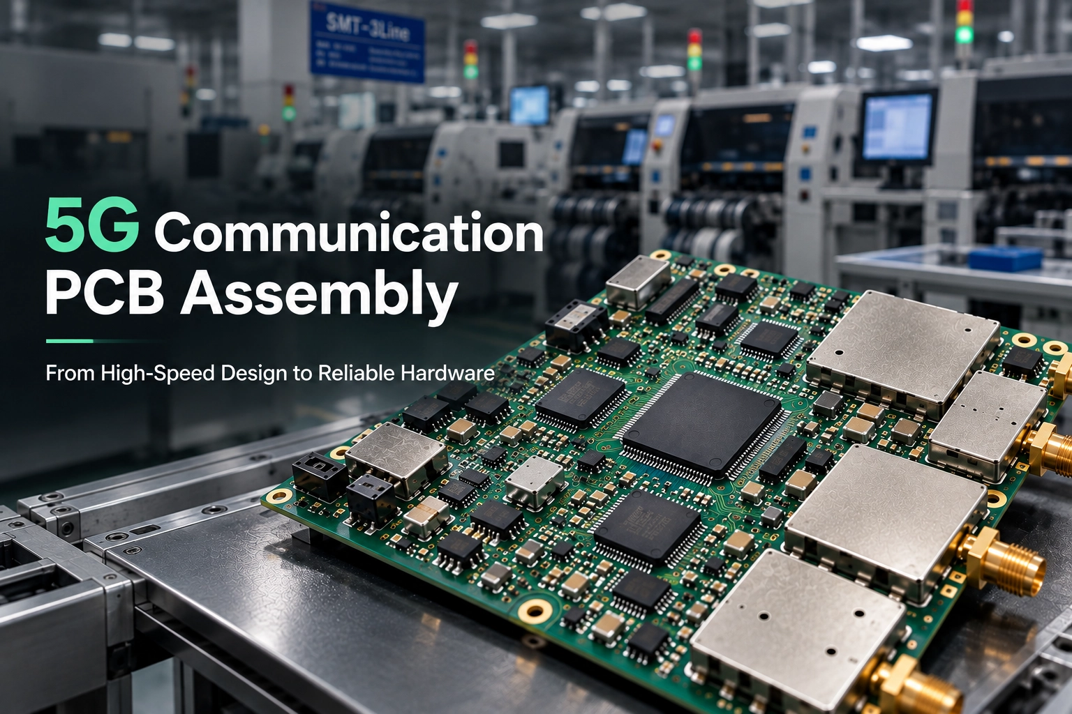
Millimeter-wave communication has the challenge of rapidly attenuating signals. Consequently, PCB antennas have to be integrated on the PCB. You will read the challenges and proven solutions. The objective of this article is to provide in-depth technical information about PCB assembly to engineers and procurement managers.
High-speed PCB assembly requires measures to maintain signal integrity. However, signal integrity can be affected by a number of factors, including the variability of the PCB fabrication process and the thickness of the solder mask.
Variability in PCB materials and the fabrication process alters the local dielectric constant and, therefore, impacts the integrity of signals at millimeter-wave frequencies.
Like other PCB assembly processes, the volume of solder paste placed on the stencil introduces variability in the assembly process that negatively impacts 5G communication PCBA. In addition, the base material used in PCBs also affects signals at higher frequencies.
Improving manufacturing control reduces variability of the high-frequency PCB assembly process. Because variability is a major challenge, selecting the right materials and processes is critical for PCB manufacturing and assembly.
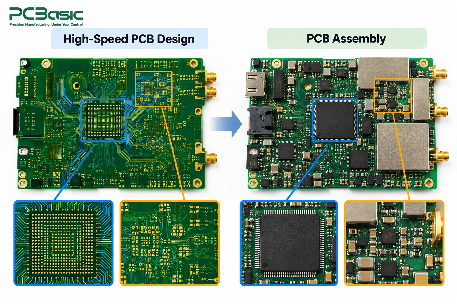
Variability in the PCB fabrication process can also impact the final design. Variations in the PCB etching process, for example, can change the thickness and width of PCB traces and other features. Variability during the PCB fabrication process can also negatively impact the spacing of PCB traces. High precision in the etching of PCBs is important to realize the desired impedance of PCB traces.
In addition, via stubs lead to unwanted reflections in high-frequency signals. To remedy this, engineers introduce either blind vias or back-drilled via structures. Fabrication of these special via types, however, increases the cost of the PCB and requires tighter process control during fabrication. Delamination of the PCB is avoided by controlling material handling, moisture, lamination, and thermal processing. Delamination reduces the reliability of the PCB over time.
Additionally, the popcorn effect during reflow is caused by moisture absorbed by moisture-sensitive components. Moisture is sometimes difficult to remove and can cause issues throughout the 5G communication PCB assembly production process. For moisture-sensitive PCBs and components, we reduce moisture by baking the PCBs prior to production when required.
Reducing the size of the components used in 5G module PCBAs necessitates the use of thinner electroformed stencils for SMT. This presents challenges for stencil design and other aspects of 5G module PCB assembly. One of the challenges is ensuring that solder paste does not spread to other areas of the stencil.
Fine-pitch assembly requires precise solder paste deposition and component placement. With SMT capabilities covering 01005/0201 components and BGA/QFN packages down to approximately 0.3–0.4 mm pitch, PCBasic can support the dense layouts found in high-speed communication hardware.
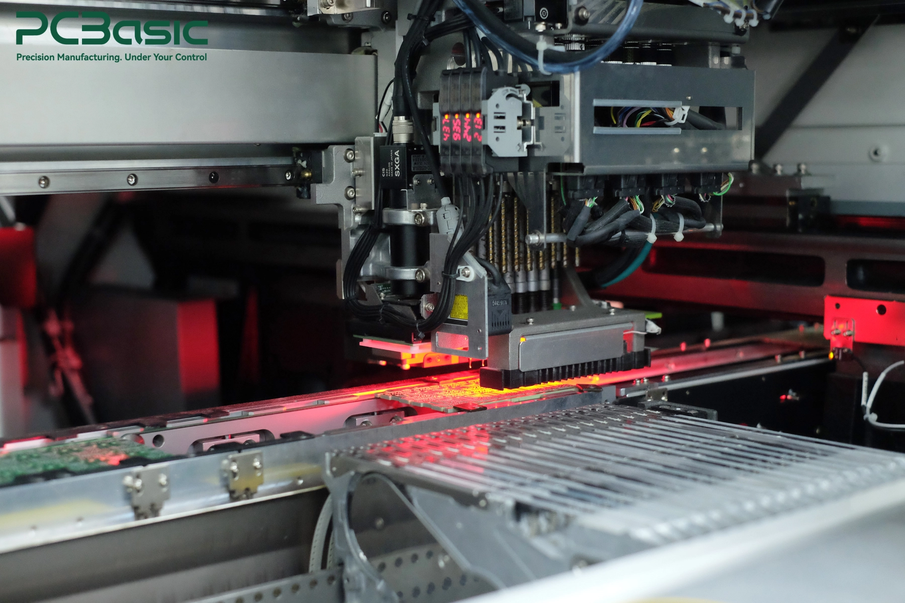
Trapped gases under thermal pads often cause voids in solder joints. In some circumstances, voiding can result in increased thermal resistance. It becomes evident that in the world of 5G, thermal management is of crucial importance.
Solder reflow can also be improved using vacuum reflow ovens. In such a case, the vacuum immediately removes gases from the molten solder and improves wetting. This is of utmost importance in assembling PCBs with fine-pitch components.
It is also important to control the time and temperature during the solder reflow in order to avoid under-soldering or over-soldering the joints. Thermal management determines the success of assembling a 5G PCB.
The similar concept of shielding can also be applied to other components in an RF system. During PCB assembly, it is of utmost importance that all connections be aligned in order to prevent leakage of EMI.
Automated systems are used for alignment prior to reflow. Likewise, the Coplanarity of Shielding cans during PCB assembly must be strictly controlled in order to prevent EMI leakage. The amount of solder fillets determines the mechanical strength of shielding cans. During drop testing of PCBs, shields must be securely attached. From a mechanical standpoint, shields must also be secured in order to prevent failure of the PCB during usage. It is essential that both requirements be met in order to successfully achieve a functional RF PCB.
SPI enables early detection of defects before they replicate. Three-dimensional SPI systems measure the volume, area and height of solder paste. This allows us to identify potential defects and ensure baseline quality of the PCB.
Tombstoning of small resistors is one defect that SPI helps to reduce by identifying uneven solder paste deposits. This is crucial in 5G PCB assembly to prevent defects from being replicated. Laser triangulation, which is an enhanced form of SPI, is used to create a topographical map of the solder paste.
SPI helps in preventing defects. This, coupled with analysis of SPI data, helps us enhance our high-density PCB assembly.
AOI is used to check the presence and polarity of components placed on the PCB. AOI systems incorporate high-resolution cameras to capture defects at the microscopic level. Incorporating learning from a ‘golden board’ helps in eliminating false defect calls.
AOI helps identify a number of defects, including solder bridges and misaligned components. This is instrumental in high-density PCB assembly. Additionally, recent advances in Artificial Intelligence and Machine Learning help AOI systems eliminate a large number of false defect calls, thus increasing line throughput and overall equipment effectiveness.
Ball Grid Arrays (BGAs) utilize an advanced interconnect package which results in a small form factor but also conceals the solder joints. Various methods exist to diagnose these joints. X-ray inspection and Computed Tomography (CT) are two such methods. CT creates a full image of the joint and is typically used for metallic interconnects.
There are strict standards for the electronics manufacturing industry. The system provides accurate measurements of voids. Cross-sectional X-Ray analysis is performed on 5G communication PCBAs to verify interconnect reliability.
To meet the reliability requirements for interconnects, the void ratio is controlled according to the package type, applicable standards, and customer requirements. CT analysis is used to study interconnect conditions before and after thermal reliability testing. The observations from this analysis can help determine whether premature failure of the product is related to interconnect or design issues.
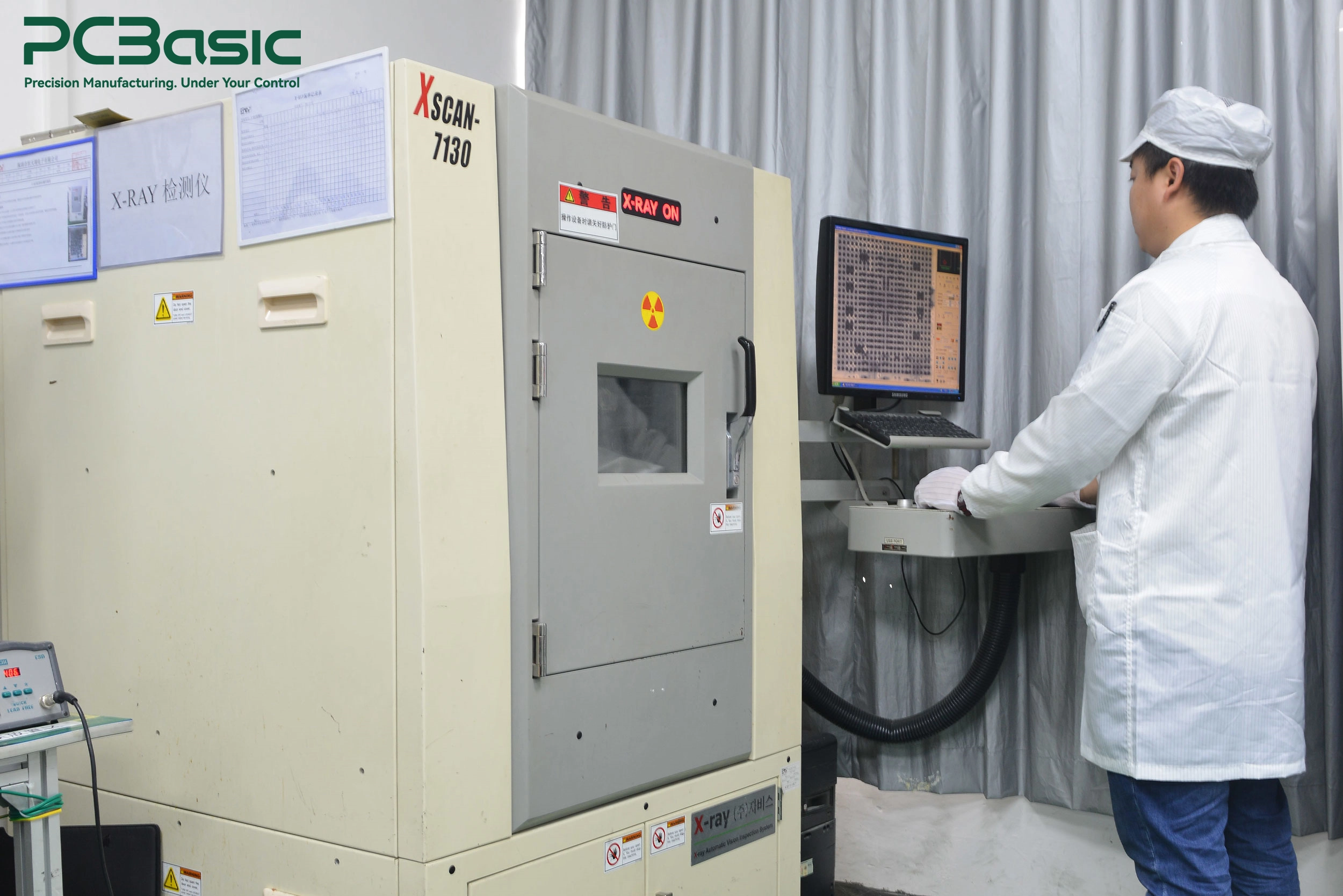
No single inspection method can identify every assembly defect. PCBasic combines SPI for solder paste inspection, AOI for visible assembly defects, and 3D X-ray for hidden solder joints. These complementary methods help identify manufacturing issues at different stages of high-density PCB assembly.
|
Inspection Stage |
Technology Used |
Primary Defect Detected |
|
Pre-placement |
3D SPI |
Insufficient or bridged solder paste |
|
Post-reflow |
2D/3D AOI |
Missing, shifted, or tombstoned parts |
|
Final stage |
3D X-Ray |
BGA voids, hidden shorts, or opens |
5G PCBAs require high-frequency and high-speed interconnects. CT and X-ray analysis can be important for rapid prototyping of these PCBs, especially when hidden solder joints are involved.
Flying probe testers check electrical paths for continuity, opens, and shorts. This establishes a baseline for further testing of high-speed PCBs.
Functional testing is performed on a populated PCBA to evaluate if the PCBA functions as designed. PCBA functional testing does not guarantee individual component values are correct. The measurement of individual component values can be performed using ICT. The measurement of digital interconnects is the responsibility of boundary scan.
The value added by ICT is evident when PCBA bed-of-nails test fixtures are used to detect opens, shorts, and selected component faults. Vectorless testing can be used to detect connection faults on IC pins and other components without requiring functional test vectors. Functional testing ensures the 5G module PCBA works without any flaw for the customer.
For electrical and functional verification, PCBasic supports flying probe testing, ICT, and FCT according to project requirements. These tests help identify connectivity problems and verify defined board functions before shipment.

The measurement of high-speed and RF signal performance requires the definition of other parameters, such as EVM and S-parameters. The measurement of the BER of the transmitted signal helps evaluate signal integrity and reliability in the presence of noise.
These parameter tests help verify that the high-speed 5G PCB assembly meets its specified signal-performance requirements. Shielded RF test chambers help achieve accurate measurement of RF signals by reducing interference from external EMI.
Multiple test methods are utilized to ensure that each unit of the customer's PCB assembly functions according to its specified electrical, functional, and communication requirements.
5G communication PCB assembly design issues often become apparent during the assembly process. Engineers need to ensure routing clearances and pad sizes. Sometimes, issues can be hidden by design decisions that are not clear to the average engineer, like the presence of sharp edges. Fortunately, there are design for manufacturing (DFM) tools to help find these issues automatically.
We evaluate the design for manufacturing and assembly (DFMA) and identify the possible issues. This helps align the design within the constraints of the manufacturing process. Often, this helps address design choices made during the PCB assembly process to reduce costs.
When this happens during the 5G PCB assembly process, it eliminates the need for more costly changes to be made later.
During a pilot production run, a small volume of PCBAs is manufactured in order to verify the integrity of the processes for high-volume PCB assembly. Many 5G PCBA designs contain a large bill of materials, which increases the cost of production. For a high first-pass yield, the process parameters of the stencil printing and reflow processes need to be carefully tuned.
Through the use of advanced analytics, modern factories gain visibility into process variation and trends that cause yield loss. These trends can be addressed by making changes to the design for process control of PCB assembly processes. We ensure these changes are made before full-volume 5G PCB assembly.
To track material traceability, we can pinpoint material failures. Unique board identification combined with MES production records helps provide end-to-end traceability.
An automated digital system records process data and maintains a digital supply chain for 5G communication PCBA.

Reliable 5G communication PCB assembly requires more than a well-designed board. Precise assembly, appropriate inspection, and consistent process control all play a role in turning high-speed designs into production-ready hardware.
Do you need reliable hardware for your next project? Contact PCBasic to get started!
Q1: What is the role of 3D X-Ray inspection in the manufacturing of 5G boards?
Designs of many high-density 5G products comprise Ball Grid Arrays (BGAs) and other packages with hidden solder joints. Utilizing 3D X-Ray inspection aids in the identification of solder defects (e.g. voids and open circuits) in BGAs. 3D X-Ray inspection, thus, enhances the overall integrity and the reliability of high-speed Printed Circuit Boards (PCBs) in 5G product platforms.
Q2: How does PCBasic achieve component traceability?
Incorporation of cutting-edge Manufacturing Execution Systems (MES) and the Internet of Things (IoT) enables component traceability. Upon evaluation, the aforementioned systems and integrated technologies enable full traceability of materials and help with quality control throughout the production and assembly of 5G communication devices.
Q3: What are some of the ideal substrate materials for 5G boards?
Suitable substrate materials are those with low-loss characteristics. For example, some of the Teflon- and Rogers-based substrates may be suitable. Identification and use of the appropriate substrate materials enhance the performance and reliability of 5G PCBs.
Assembly Enquiry
Instant Quote


Phone contact

+86-755-27218592
In addition, we've prepared a Help Center. We recommend checking it before reaching out, as your question and its answer may already be clearly explained there.
Wechat Support

In addition, we've prepared a Help Center. We recommend checking it before reaching out, as your question and its answer may already be clearly explained there.
WhatsApp Support

In addition, we've prepared a Help Center. We recommend checking it before reaching out, as your question and its answer may already be clearly explained there.
