
Global high-mix volume high-speed PCBA manufacturer
9:00 -18:00, Mon. - Fri. (GMT+8)
9:00 -12:00, Sat. (GMT+8)
(Except Chinese public holidays)





HomePage > Blog > Knowledge Base > Bluetooth Module PCB Assembly: SMT Challenges and Production Testing
1. What Makes Bluetooth Module PCB Assembly Different?
2. Fine-Pitch SMT Assembly Challenges and Process Control
3. Inspection and Quality Control in Bluetooth PCB Assembly
4. Production Testing for Bluetooth Module PCBA
5. From Prototype PCB Assembly to Consistent Bluetooth Module PCBA Production
A Bluetooth
module that works flawlessly on the bench will sometimes lose connection when
it hits the market. The root cause is not always found in the firmware. The
problem is more likely a slight change in solder paste volume or misplaced
matching part that affects RF performance. It’s not until a customer complains
about range that someone catches on. Bluetooth module PCB assembly bridges the
gap between a successful prototype and a repeatable product.
Demand constantly drives up volume. According to ABI Research, global shipment of Bluetooth devices will increase from approximately 5.4 billion units in 2025 to over 8 billion units in 2030. For devices using Bluetooth PCB modules, each module has to function in the same way for unit ten thousand as unit ten.
In this article, you will learn about factors that differentiate Bluetooth module PCBA from normal electronics assembly, factors affecting process control due to fine-pitch SMT assembly and RF sensitive areas, test requirements for both inspection and manufacturing processes, and how projects are taken from prototype to volume.
The Bluetooth PCB module comprises a radio, antenna or antenna interface, and other circuits on a printed circuit board which is much smaller than a postage stamp. The combination of this high density and the RF sensitivity makes wireless module PCB assembly different from conventional digital board assembly.
Most Bluetooth devices contain a wireless SoC, a crystal, a matching circuit, a power circuit, and an antenna, which is either a PCB trace antenna, a chip antenna, or an external antenna connected through an RF connector. In some designs, a radio-frequency shielding can is included.
Each of the above components presents its own challenge to the line. Proper placement and joint quality are required to maintain crystal frequency stability, and small matching passive components require very tight placement tolerances. Castellated or LGA components require controlled solder volume to allow the module to mount flat on the host PCB. A Bluetooth PCB assembly that does not properly consider the needs of the above components will exhibit problems in terms of erratic performance and range.
The antenna section of a Bluetooth module PCBA poses a much greater challenge than the other sections of the board because the keep-away region around the antenna must follow the specified restrictions on copper, components, or solder residues as they could affect the resonant frequency of the antenna and reduce its range.
Process control is even more critical at this point as a small change like different flux residue, or solder mask thickness could change the behavior of the antenna. This is why it requires much stricter process control than other digital boards where wireless modules need to be installed.
Host board design represents another variable factor as an identical module mounted on a board close to a metal case, battery or big ground area will perform differently compared to the same module mounted on the test board.

Most Bluetooth PCB assembly work happens on the SMT line, and that is also where most hidden risk enters the product.
The careful review of the BOM precedes any application of the paste on the board. RF matching parts, crystals, and the module SoC have certain values and tolerances. An unapproved substitution of an almost identical component may affect RF performance without causing an obvious visual defect.
Moisture-sensitive components need to be treated with extreme care. During the reflow soldering process, moisture-sensitive modules and SoCs that have exceeded their permitted floor life after removal from dry packaging may crack or delaminate. PCBasic does DFM reviews and BOM checks before production, which allows issues to be investigated before they become expensive.
Sourcing is equally important. Using RF parts and modules purchased from authorized sources reduces the risk of counterfeit parts, which may cause unexpected range and frequency problems.
Fine-pitch SMT assembly defines the difficulty of a Bluetooth module PCB assembly project. The components that have QFN and LGA packages, 0402 and 0201 passives, and small pad spacings give very little tolerance in terms of stencil and placement accuracy.
The stencil aperture is what dictates the amount of paste to be deposited on every pad. Too little paste may result in open solder joints while too much may create bridges between neighboring pads. In addition, a larger thermal pad is prone to entrap voids that affect the efficiency of heat transfer.
The reflow profile should be such that it would sufficiently heat up the PCB but not stress the crystal or the plastic and metal components of the module itself. PCBasic runs SMT assembly with fine-pitch component placement for these dense layouts, with process checks built into each stage.
Matching components are placed between the radio and the antenna, and they only function when the value and placement of these components match the design specifications. If the capacitor is misplaced slightly off the pad or there is too much solder at the joints, it may alter the RF circuit's parasitic characteristics or affect solder joint reliability.
The shield cans are another variable that we have to deal with. If a can is misaligned or soldered to an adjacent pad, it can create a short in the signal or change the tuning of the trace near it.
Inspection catches assembly defects before they turn into field returns, and the right mix depends on the module's design.
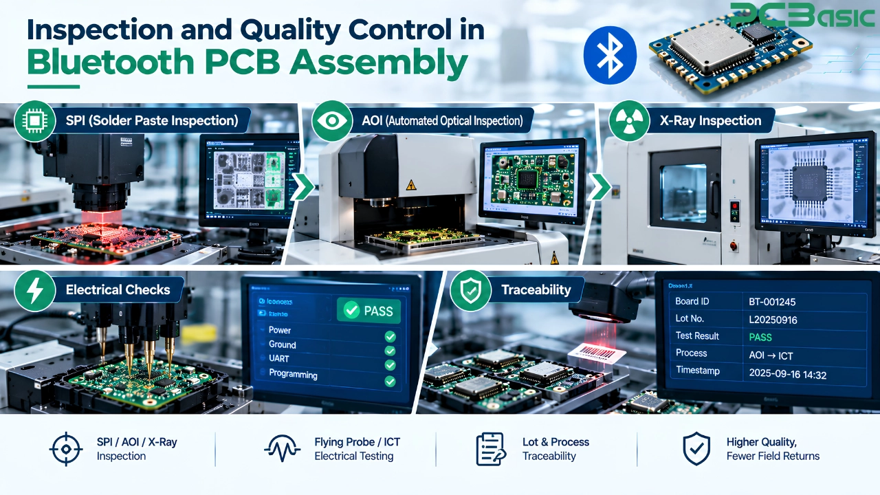
Solder paste inspection checks the volume and placement of paste right after printing. Paste problems are the most common source of fine-pitch defects, so catching them before any component is placed saves rework. Automated optical inspection inspects placement, polarity, and the visible solder joints after reflow soldering.
Hidden solder joints require a different kind of inspection tool. Inspection by X-ray is useful because some modules have LGA pad areas or shielded areas that restrict the optical inspection process.
Not all Bluetooth modules require all types of inspection tools. A basic module having exposed castellated pads might not use the 3D X-ray but the SPI and AOI instead. PCBasic provides SPI, AOI, and 3D X-ray services, and it customizes the inspection process based on the requirements of the board.
Bluetooth module PCBA inspection is not limited to the physical inspection only. Flying probes are a good option for prototyping and low-volume production without using fixtures, whereas ICT is a better choice when dealing with high-volume production when suitable test points are available on the board. Design for test comes in handy in this situation – availability of pads for power, ground, UART, and programming allows reliable contact of the fixture with the board, thus reducing time and assuring repeatability.
Traceability allows linking every single test result to a particular board. In case of defect discovery, information about lots and processes allows identifying other boards with the same defect source rather than making assumptions. Traceability is incorporated in the PCBasic manufacturing process.
A module can look flawless and still fail to connect. Production testing confirms that each unit actually works as a Bluetooth device.
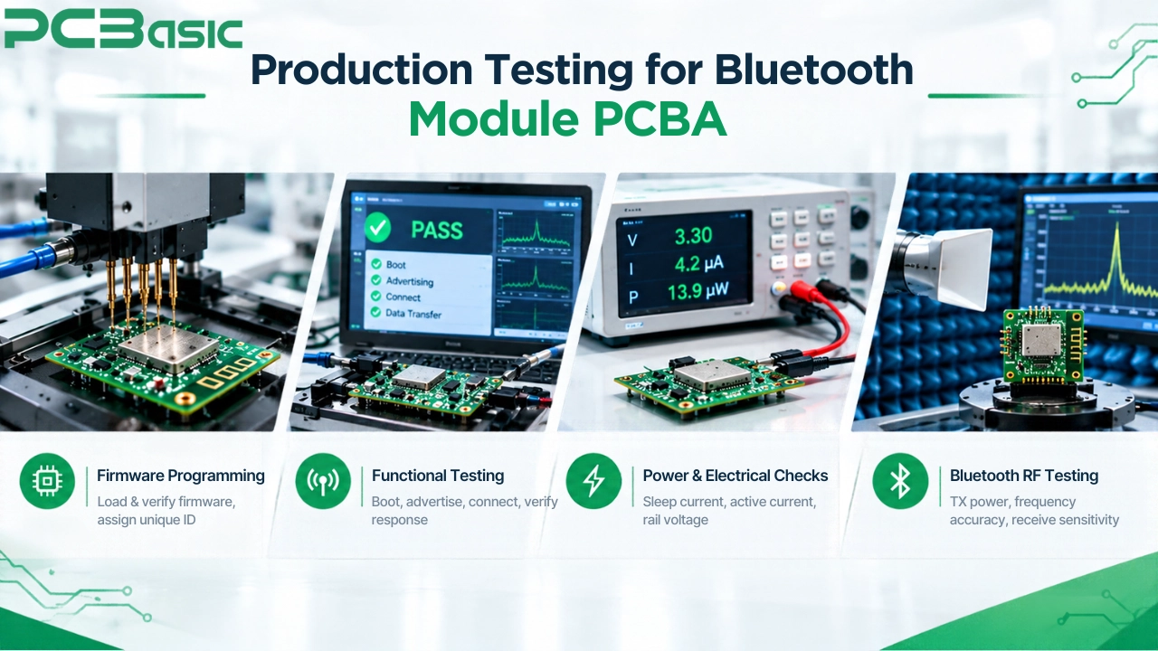
Firmware programming usually comes first, often through test pads or pogo pins that reach the programming interface. A verification step then confirms the code loaded correctly, since a partial or corrupted write can pass a quick check and fail later in the field. Many programs also write a unique identifier or address to each module at this stage, which makes traceability and later support much easier.
Bluetooth functional testing then confirms the module boots, advertises, and responds as expected. PCBasic supports PCBA functional testing and test-fixture-based verification built around the customer's own test procedure, so the checks that matter for each product run on every unit.
Power behavior is often more telling than connectivity testing in many ways. Sleep current, active current, and rail voltage are clear indicators of power behavior.
A module that connects well but consumes more current while in sleep mode can drain batteries in weeks rather than years. RF performance depends on crystal frequency and supply stability as well, thus making these electrical measurements useful for both radio and battery performance.
Bluetooth RF testing tests the radio circuitry directly. Common tests include transmit power, frequency accuracy, and receive sensitivity, performed using appropriate conducted or over-the-air test setups, often with RF shielding to reduce external interference.
Depending on the test method, Bluetooth module testing at this level can help identify RF performance issues, including antenna detuning and matching problems that cannot be detected by visual inspection alone. Adding a simple connect test using a reference unit is an additional test that proves the module will pair and maintain a connection.
The level of testing required should be appropriate to the application. The testing of a simple beacon module would have a completely different set of tests than a Bluetooth module incorporated into a medical wearable device.
A handful of working samples does not prove that Bluetooth module PCBA manufacturing will stay stable at volume.
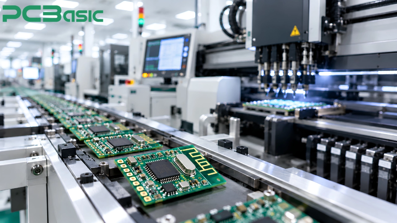
Prototype PCB assembly is the first opportunity to identify issues related to design and manufacturing processes. First Article Inspection then verifies the first article produced against the drawings, BOM, and test requirements prior to going into volume.
In a single step, the stencil, reflow profile, placement program, and test fixture can be validated.
Any engineering changes need equal consideration. If the change replaces a component or changes a matched value, having a change process and a quick re-validation prevents the modification from causing yet another problem. Finding an issue with the paste application or placement on the first article is much cheaper than discovering that issue after manufacturing thousands of boards.
Once production has started, consistency is achieved by controlling factors that can cause variation. Consistency is improved through use of approved components, set process parameters, and documented test results.
PCBasic supports the full path from prototype to production, with first article inspection, MES traceability, and manufacturing records that tie each board to its components, process data, and test results. That record gives a customer a clear answer if a field issue ever appears.

The Bluetooth module PCB assembly is successful if the SMT process, the inspection strategy, and the production tests are aligned with the realities of an RF device. Fine-pitch devices, delicate antenna zones, and small matching components do not allow for any guessing games, and each step either preserves the radio performance or destroys it silently.
PCBasic offers Bluetooth module development support for DFM review and BOM validation right through to SMT assembly, inspection, functional test, and prototype to production control. Should your next wireless device require a partner that appreciates how different these boards are, we would love to hear from you.
Q1: What is Bluetooth module PCB assembly?
It is the process of manufacturing a board comprising a Bluetooth radio, antenna or antenna interface, and associated circuitry, with precise SMT so that the module can function reliably in mass production.
Q2: Why does fine-pitch SMT assembly matter for Bluetooth modules?
QFNs and LGA are examples of dense packages that will not tolerate paste or alignment errors. This is because very small errors may detune the RF section without leaving any visible signs.
Q3: Does every Bluetooth module need X-ray inspection?
No. Simple modules with exposed pads may rely on SPI and AOI, while designs with hidden joints under LGA pads or shields benefit from X-ray inspection as well.
Q4: What does Bluetooth RF testing check?
It typically checks transmit power, frequency accuracy, and receiver sensitivity, often in a shielded fixture, to confirm the radio and antenna behave as designed.
Q5: How should a Bluetooth module move from prototype to production?
Start with prototype assembly, validate the process with a first article inspection, and then lock approved components, process settings, and traceability records before ramping to volume.

Assembly Enquiry
Instant Quote



Phone contact

+86-755-27218592
In addition, we've prepared a Help Center. We recommend checking it before reaching out, as your question and its answer may already be clearly explained there.
Wechat Support

In addition, we've prepared a Help Center. We recommend checking it before reaching out, as your question and its answer may already be clearly explained there.
WhatsApp Support

In addition, we've prepared a Help Center. We recommend checking it before reaching out, as your question and its answer may already be clearly explained there.
