Global high-mix volume high-speed PCBA manufacturer
9:00 -18:00, Mon. - Fri. (GMT+8)
9:00 -12:00, Sat. (GMT+8)
(Except Chinese public holidays)
Global high-mix volume high-speed PCBA manufacturer
9:00 -18:00, Mon. - Fri. (GMT+8)
9:00 -12:00, Sat. (GMT+8)
(Except Chinese public holidays)
HomePage > Blog > Knowledge Base > What are Blind and Buried Vias?
These features are quite important in the manufacturing of HDI PCBs as these PCBs serve as the basis for many technologies used in telecommunication, automotive, aerospace, and medical equipment.
Let’s take a dive into this article and understand how important these vias are for advancement in PCBs and how they can play their part in driving the success of modern electronic systems.

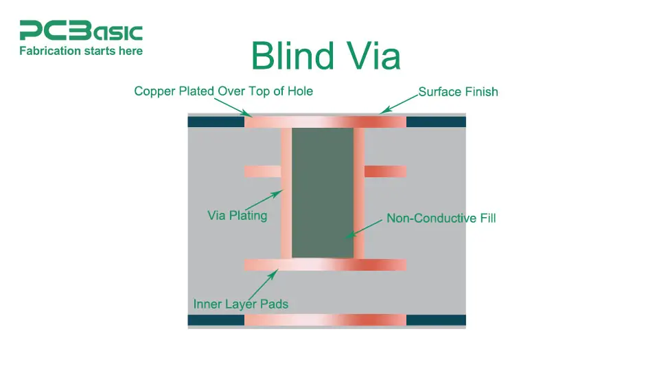
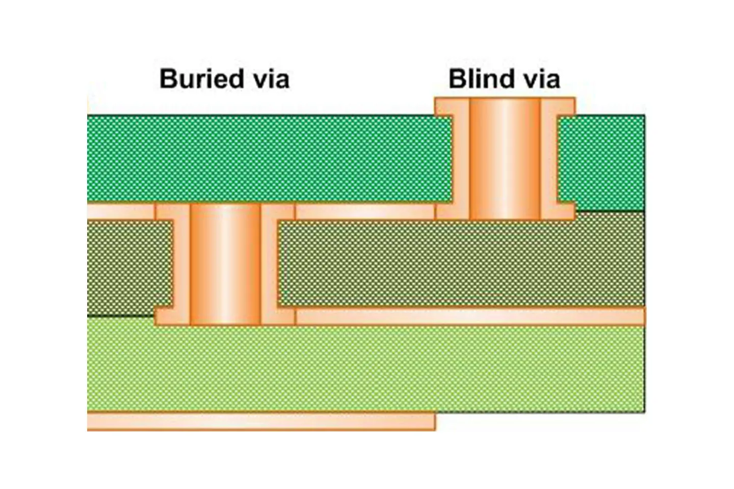
Blind vias are one of a type that makes PCB layers interconnected while ensuring it stay compact and can have advanced functionalities. It is an important process in the designing and manufacturing of multilayer PCBs. A blind via can connect the outer layer of the multilayer to at least one inner layer without going through the entire thickness of the board. This feature separates it from other types such as through hole and a buried via which joins only the inner layer, unlike blind vias.
Blind vias are quite nessasy in HDI Pcbs. In the evolution of electronics, one important factor that is making things modern is the compactness of electronics. Unless PCBs can't be compact the final product won't end up compact so blind vias play an important role in making PCBs compact as well as high performance.
Even the more complicated circuit layout and miniaturization of electronic apparatus enables without influencing its performance or dependability by incorporation of blind vias. Now let's take a look at its main characteristics, benefits in using PCBs, and some disadvantages as well to make things clear why this tech is important in multilayer PCBs.
Blind vias do have some important characteristics that ensure their indispensability for advanced PCBs:
● Partial Depth Drilling: Blind vias do not go through the PCB completely but can connect one of the PCB outer layers to several inner layers which can be terminated within the PCB board structure. The depth of this vias is controlled to match the particular layers it connects.
● Smaller Diameters: The diameters of blind vias are mostly less than 0.15mm, which is quite small, which makes them suitable for HDI compact layouts that have higher density. It plays an important role in making PCB compact.
● Advanced Drilling Techniques: For drilling methods like laser drilling or mechanical drilling should be followed in blind vias. Laser drilling offers a precise method of drilling small diameter vias without making any damaged material in the vicinity which makes it more preferable.
● Layer-Specific Connectivity: Blind via offers specific layer interconnections that reduce the chances of signal stubs, which improves electrical performance in high-frequency circuits.
Here’s some advantages of Blind Vias offers in PCB Design:
● Space Optimization: Blind Vias offers space-efficient design on Multilayer PCBs which is important in modern electronics. This space can be utilized for accommodating more components or making the PCB compact itself. PCBs with blind vias can be used in compact devices like smartphones and wearables.
● Improved Signal Integrity: since bling vias avoid unnecessary via stubs they do not allow signal reflections which improve the performance of high-frequency circuits. So this utility can applied for applications that involve faster transmission of signals, like telecommunications and data processing.
● HDI Technology Support: As their design can support compact layouts the blind vias are ideal for HDI PCBs. They can accommodate multilayer boards with high component density.
While there are some major advantages related to blind vias, there are also some drawbacks and issues:
● Higher Manufacturing Costs: with the requirements of advanced drilling techniques like laser drilling and sequential lamination, which are more expensive than standard through-hole vias blind vias have quite higher manufacturing costs.
● Complex Fabrication Process: Blind vias have partial drilling requirements and the need for accurate layer alignment that can raise the fabrication complexity, and increase production time and chances of defects.
● Reliability Issues: Poor fabrication of blind vias might result in defects like voids, lack of plating, or thermal stress cracks which can deteriorate the electrical and mechanical integrity of a PCB.
● Design Limitations: Even though blind vias allow for a great deal of design flexibility, designs are still strictly bound by particular design rules, like minimum via size and aspect ratio, which sometimes can affect manufacturability or performance.

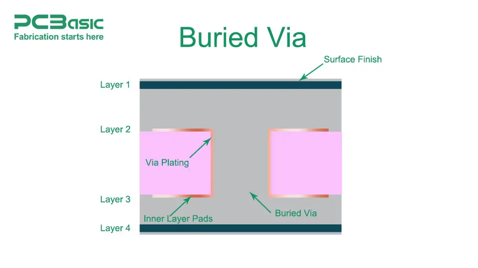
Buried vias are a special kind of visa used in multilayer PCBs for connecting two or more internal layers without reaching either outer surface of the board. Such vias are enclosed within the structure of the PCB and thus are not visible. Buried vias are becoming indispensable in advanced PCB designs, especially in HDI boards, where space limitations and performance imperatives are driving the need for better interlayer connectivity.
Buried vias are critical in the development of compact, reliable, and high-performance electronic systems. Allowing internal connections while leaving the surface layers free for component placement and routing, buried vias maximize the functionality and density of modern PCBs. Let's look at their key features, along with their pros and cons, in detail.
The distinguishing features of buried vias include a number compared to other vias:
● Internal Layer Connection: Vias buried join only the inner layers. In fact, in the board's structure during lamination, completely enclosed structures don't reach out to the outermost layers.
● Advanced Manufacturing Techniques: In buried vias the process used is called successive lamination where in the inner layers are fabricated and then laminated on the board before the vias are drilled. While maintaining strong interconnection this can provide the ability for accurate alignment.
● Layer-Specific Functionality: Sometimes, blind vias connect certain internal layers. This gives a designer the ability to create an isolated signal path or power plane without encumbrances on the surface layers.
● Miniaturization: Being normally of small diameter, buried vias are easier to use in high-density complex applications. They contribute to compact and effective PCB layouts, especially in gadgets like smartphones, medical devices, and automotive electronics.
All of these features make buried vias irreplaceable for designers who have to fight in complex and space-limited projects of printed circuit boards.
The integration of buried vias in PCB design offers several benefits that enhance performance, functionality, and design efficiency:
● Space Optimization: As buried vias connect only internal layers, the surface real estate is freed. This gives options for traces to route and components to mount on outer layers better, which is very important in compact devices.
● Improved Signal Integrity: The buried via aids in signal isolation within the PCB, reducing crosstalk and EMI. This is very important in high-frequency designs where signal integrity cannot be compromised.
● Improved Layer Utilization: Buried vias enable better use of internal layers, allowing designers to create dedicated power planes, ground layers, or signal paths without compromising the surface layout.
● Support for HDI Technology: Buried vias offer great compatibility for HDI PCBs, which are widely used in complex electronic systems. Their ability to provide interlayer connections while making sure the PCB is compact makes them great for high-density applications.
● Mechanical Strength: As buried vias are completely buried in the PCB they improve the mechanical stability of the board which reduces the risk of damage during assembly or operation.
Despite the advantages, buried vias do have some challenges and limitations that need to be considered during design and manufacturing:
● Higher Manufacturing Costs: The manufacturing process for buried vias requires additional steps, such as sequential lamination and precision drilling, which increases production costs. This can make them less feasible for cost-sensitive applications.
● Complex Manufacturing Process: Buried vias need high-tech equipment and expertise to manufacture. The sequential lamination process complicates the manufacturing workflow, increasing the chances of errors and lengthening production times.
● Inspection and Testing Challenges: As buried vias are invisible externally, quality testing demands specialized tools like X-ray imaging, adding cost and complexity.
● Design Constraints: Designers must adhere to strict rules regarding size and aspect ratio, limiting design flexibility.
● Thermal Stress Concerns: Poorly fabricated buried vias may fail under thermal stress, compromising reliability in high-temperature environments.
Buried vias are integral to modern PCB design, enabling high-density and high-performance circuits that meet the demands of today’s advanced electronics.

● HDI PCBs: These vias are fundamental in high-density interconnect boards, enabling compact layouts for devices like smartphones, tablets, and wearable technologies.
● Automotive Electronics: They are employed in advanced driver-assistance systems (ADAS), infotainment systems, and other high-performance automotive components.
● Medical Devices: Buried and blind vias support miniaturized medical equipment, such as implantable devices and diagnostic tools, by providing compact and reliable circuitry.
● Aerospace and Defense: Rugged, space-constrained designs for systems used in aerospace and defense are possible with the use of buried and blind vias.
● Telecommunication Equipment: Devices like routers, servers, and base stations rely on buried and blind vias for high-frequency and high-speed signal transmission.
The complexity of including blind and buried vias in PCB manufacturing significantly affects costs. Key cost factors include:
● Advanced Manufacturing Processes: Fabrication requires sophisticated techniques like laser drilling and sequential lamination, driving up production expenses.
● Material Usage: Additional materials, such as resin-coated foils and prepregs, may be needed to support advanced structures.
● Design Complexity: Precise alignment and layer registration add to both design and manufacturing costs.
● Testing and Inspection: Ensuring the reliability of these vias necessitates advanced testing methods, further increasing costs.
While more expensive than standard through-hole vias, the advantages they offer in terms of space optimization, performance, and design flexibility often justify the investment, particularly in high-end and mission-critical applications.
In addition to blind and buried vias, through vias and micro vias are widely used in PCB manufacturing, each serving distinct design purposes.
Through vias are most conventional type of vias in PCB design. They extend through the entire thickness of the PCB, connect all layers from the top to the bottom.
● Key Features: Created using mechanical drilling, through vias are generally larger than blind or micro vias.
● Applications: Through vias are cost-effective and suitable for simpler, low-density PCB designs. However, they can occupy valuable routing space on outer layers, making them less ideal for compact or HDI designs.
Micro vias are small vias typically created using laser drilling. They connect adjacent layers or span up to two layers, making them ideal for HDI PCBs.
● Key Features:
○ Diameter of less than 150 µm.
○ Limited to connecting a few layers, enhancing routing density.
○ Manufactured using advanced processes like laser drilling.
● Applications: Microvias are extensively used in high-frequency, high-density designs, such as smartphones, wearable devices, and other compact electronics.
While micro vias and blind vias have some similarities, they also have some significant differences which significantly in functionality and applications:
● Size: Compared to blind vias micro vias are smaller which makes them a good fit for ultra-compact designs.
● Layer Connectivity: Micro vias can connect adjacent layers, whereas blind vias can link outer layers to internal ones.
● Manufacturing Complexity: It needs laser drilling in micro vias while blind vias can use both laser or mechanical drilling which depends on what kind of requirements are.
● Cost: Comparatively speaking micro vias are more expensive than blind vias because of their size and precision.
Blind and buried vias are quite important features now in modern PCB manufacturing. To meet the demands of advanced electronic devices these features enable compact, high-performance, and intricate designs in PCBs. These specialized vias provide designers the flexibility to optimize space, better signal integrity, and support high-density interconnect HDI applications.
While blind and buried vias have many advantages they also have some drawbacks like adding complexity and cost related. These kinds of multilayer vias PCBs are very useful in industries where precision and performance matter, like in telecom, automotive, aerospace, and medical devices.
We, PCBasic, specialize in producing state-of-the-art PCBs that utilize advanced technology to achieve exceptional results. Whether you require HDI boards with complex configurations or standard multilayer designs, our expertise guarantees top-quality performance for your applications.

Assembly Enquiry
Instant Quote
Phone contact

+86-755-27218592
In addition, we've prepared a Help Center. We recommend checking it before reaching out, as your question and its answer may already be clearly explained there.
Wechat Support

In addition, we've prepared a Help Center. We recommend checking it before reaching out, as your question and its answer may already be clearly explained there.
WhatsApp Support

In addition, we've prepared a Help Center. We recommend checking it before reaching out, as your question and its answer may already be clearly explained there.