Global high-mix volume high-speed PCBA manufacturer
9:00 -18:00, Mon. - Fri. (GMT+8)
9:00 -12:00, Sat. (GMT+8)
(Except Chinese public holidays)
Global high-mix volume high-speed PCBA manufacturer
9:00 -18:00, Mon. - Fri. (GMT+8)
9:00 -12:00, Sat. (GMT+8)
(Except Chinese public holidays)
HomePage > Blog > Knowledge Base > BJT VS. MOSFET: What is the Difference?
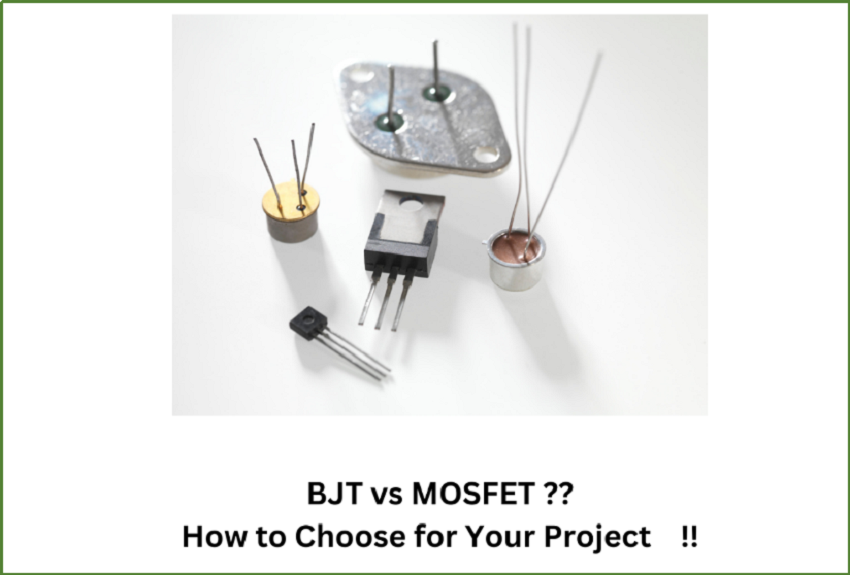
In every electronics design project, the choice of the transistor can make or break your project. Bipolar Junction Transistors (BJT) and Metal-Oxide-Semiconductor Field-Effect Transistors (MOSFET) are two commonly used transistors in electronic circuits. Although both types can be used for amplification and switching their underlying principles and applications significantly differ from each other.

Here we are going to break down the differences, strengths, and weaknesses of both BJTs and MOSFETs. We will guide you on how to choose the right transistor for your electronics design project. By the end, you'll understand where to use each and why.
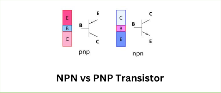
A Bipolar Junction Transistor (BJT) is a current-controlled device that amplifies or switches electrical signals. It comprises three doped layers of semiconductor material, with two junctions formed within a transistor. Layers in a BJT are referred to as:
· Emitter: A layer that supplies charge carriers.
· Base: The inner layer controls the flow of charge carriers.
· Collector: A layer that collects the charge carriers from the emitter.

The operation of a BJT circles around the current control. When a small current flows into the base-emitter junction, a large current flows between the collector and emitter. This principle is usually referred to as current amplification. The base acts as a regulator, hence controlling the collector-emitter current.
· Flow of electrons (in NPN type) or holes (in PNP type).
· Control via base current.

What Is an NPN Transistor?
NPN transistor is a type of BJT that contains a P-type semiconductor layer sandwiched between two N-type semiconductor layers.
What Is a PNP Transistor?
A PNP transistor is a type of BJT in which an N-type layer is sandwiched between two P-type layers.
· High Current Gain: This is ideal for amplifying weak signals.
· Temperature Sensitivity: Performance is more likely to degrade at higher temperatures.
· Analog Handling: Suitable for analog applications due to its linear operation.
|
Characteristics |
Common Base |
Common Emitter |
Common Collector |
|
Input Resistance |
Very Low |
Low |
Very High |
|
Output Resistance |
Very High |
High |
Low |
|
Current Gain |
Less than 1 |
High |
Very High |
|
Voltage Gain |
Greater than CC and Less than CE |
High |
Low |
|
Power Gain |
Medium |
High |
Medium |
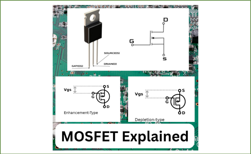
MOSFET is the short name for "Metal Oxide Semiconductor Field Effect Transistor." It is basically a voltage-controlled device that is used for both switching and amplification applications. It has three main parts described below:
· Gate: Used to control the MOSFET.
· Source: It provides charge carriers.
· Drain: It receives carriers.

In a MOSFET, there exists a thin oxide layer between the gate and the channel, which insulates and prevents the direct current flow, hence making MOSFET a highly efficient device.
A depletion-mode MOSFET is a type of MOSFET which is normally ON even at zero gate-to-source voltage (VGS). This "normally-on" characteristic enables the MOSFET to conduct current by default, just like a closed switch. In circuit diagrams, a depletion-mode MOSFET is represented by a solid channel line, which indicates the presence of an active (conductive) channel at zero gate bias.
In order to turn OFF an n-channel depletion MOSFET, we need to you apply a negative gate-to-source voltage (-VGS. This negative bias depletes the channel of free electrons, stopping current flow. In contrast, if we increase VGS in the positive direction, the channel gets more and electrons, hence, increasing the current flow.
For a p-channel depletion MOSFET, things are the opposite. When we apply a positive gate bias +VGS, it depletes the channel of holes and turns it off. While a negative gate bias −VGS will allow more current to flow.
Although depletion-mode MOSFETs are not common among designers because their enhancement-mode counterparts (which are normally off at VGS = 0), can be used in certain applications which require a device to be “ON” by default. Think of them as “normally closed” switches that you can open with the proper gate voltage.
The enhancement-mode MOSFETs are a widely used type of MOS transistors. They behave differently than depletion-mode types. In an enhancement mode, the channel is normally “OFF” when there is no gate-to-source voltage (VGS = 0 V).
In circuit diagrams, the channel is represented by a dashed line. This is an indication that the current does not flow by default.
Normally OFF: At VGS = 0, there is no path for the current to flow.
Turning ON: When VGS exceeds a certain threshold voltage VTH. Electrons are attracted to the region under the gate, creating (or “enhancing”) a conductive channel. Current can now flow from the drain to the source.
More Voltage, More Current: As you increase VGH beyond VTH, the channel becomes even better at conducting, so there are more current flows.
Switch Analogy: Think of it as a “normally open” switch—applying a positive voltage closes the switch and allows current.
Normally OFF: At VGS = 0, no current flows.
Turning ON: When we apply negative gate-to-source voltage, it creates a conductive channel by attracting holes.
The more the Negative Voltage is, the more current will be: Increasing the negative voltage will make the channel more conductive, hence allowing more current flow.
Switch Analogy: For a p-channel MOSFET, a negative voltage at the gate “closes” the switch, while a zero or positive voltage keeps the switch open.
To summarize, enhancement-mode MOSFETs start with an open channel (no conduction) and require a gate voltage (positive for n-channel, negative for p-channel) to “enhance” or create a conducting path. This is why we call them “normally open” devices: they only allow current to flow when the gate voltage is sufficiently different from the source voltage.
In a MOSFET, current flow is controlled by the virtue of an electric field. When a voltage is applied to the gate, it either increases (enhances) or decreases (depletes) the conductivity of the channel between the source and drain. This whole process relies on an electric field rather than the flow of current. MOSFETs can precisely manage currents with minimum power loss.
MOSFETs have a fast control structure. Just by varying the voltage at the gate, we can regulate how much current will flow between the source and the drain. MOSFETs are efficient and fine-tuned devices that make them a first choice for designing robust power electronics circuits.
If we Compare BJT vs MOSFET, it offers the following features:
Higher Input Impedance: MOSFET draws almost no current at the gate. This is the main reason we have reduced power consumption on the control side.
Improved High-Frequency Performance: MOSFET is a fast-switching semiconductor device. This feature makes it ideal for RF (Radio Frequency) and other high-speed applications.
Summarized are the basic characteristics of MOSFETs:
High Input Impedance: Extremely low gate current and minimum power consumption.
Fast Switching: Fast on/off control makes it suitable for high-frequency circuits.
Low Power Consumption: First choice of efficient electronics circuits.
|
Characteristics |
BJT |
MOSFET |
|
Control Mechanism |
Current-controlled |
Voltage-controlled |
|
Switching Speed |
Moderate |
High |
|
Power Consumption |
High |
Low |
|
Thermal Stability |
More sensitive |
Less sensitive |
|
Complexity of Drive Circuit |
Simple |
Complex |
Let’s compare the pros. and cons. of BJT and MOSFET amplifiers. This comparison will surely help you choose the right transistor for your project.
Strengths: Their linear characteristics make them strong candidates for audio and analog circuits where signal fidelity is very crucial.
High Current Gain: BJT amplifiers produce smooth and consistent output for audio/ low-frequency applications.
Strengths: They are the first choice for RF (radio frequency) and high-power setups due to their speed and efficiency.
Less Distortion: MOSFET Amplifiers offer extremely low distortion and maintain signal clarity at a wide spectrum, especially at higher frequencies.
Let’s define when to use MOSFET and when to use BJT in our switching applications.
Pros: BJTs are low-cost devices and are simple to use. They are suitable for many low-power tasks.
Cons: Switching speeds of BJTs are slower compared to MOSFETs. They have high power losses as well, hence deciding their rejection for efficient and fast switching circuits.
Pros: MOSFETs are ideal candidate for high-speed applications like SMPS (Switched Mode Power Supplies) and motor controllers due to fast switching and low on-resistance.
Cons: High-power MOSFETs are often costly, but their efficiency and control robustness offset the initial costs.
|
Features |
NMOS |
PMOS |
|
Charge Carries |
Electrons |
Holes |
|
Switching Speed |
Fast |
Slow |
|
On-resistance |
Low |
High |
|
Applications |
High-performance circuits |
Low-power circuits |
· If you require linearity and high current gain use BJTs like in audio amplifiers.
· MOSFETs outperform due to their fast switching and high efficiency. Best for high-frequency and high-power amplifiers.
· MOSFETS are ideal for quick on/off control with minimal power loss. They offer good thermal stability.
· BJTs are Great for simple and low-cost designs where switching frequency is moderate or not critical.
When you must decide between a BJT or a MOSFET, you should first draft your requirements. You need to first narrow down whether it will be used as a switch or an amplifier, whether the circuit is high speed or not, do we have to design an efficient circuit or just a normal control.
BJTs are ideal for analog amplification. They offer budget-friendly design, while MOSFETs outperform in high-speed and energy-efficiency applications. By comprehending the unique strengths and limitations of each, we can choose the transistor that delivers the optimized performance for your specific power electronics design project.

Assembly Enquiry
Instant Quote
Phone contact

+86-755-27218592
In addition, we've prepared a Help Center. We recommend checking it before reaching out, as your question and its answer may already be clearly explained there.
Wechat Support

In addition, we've prepared a Help Center. We recommend checking it before reaching out, as your question and its answer may already be clearly explained there.
WhatsApp Support

In addition, we've prepared a Help Center. We recommend checking it before reaching out, as your question and its answer may already be clearly explained there.