Global high-mix volume high-speed PCBA manufacturer
9:00 -18:00, Mon. - Fri. (GMT+8)
9:00 -12:00, Sat. (GMT+8)
(Except Chinese public holidays)
Global high-mix volume high-speed PCBA manufacturer
9:00 -18:00, Mon. - Fri. (GMT+8)
9:00 -12:00, Sat. (GMT+8)
(Except Chinese public holidays)
HomePage > Blog > Knowledge Base > Overview of Amplifier Circuit Diagram
Amplifiers are everywhere in modern electronics. They power the audio amplifier circuit, communication systems, and signal processors. At the core of every amplifier lies its circuit diagram — a map showing how components connect to boost signals without distorting their original waveform. So, understanding the amplifier circuit diagram is key for anyone working with electronics.
This guide breaks down how amplifier circuits work, what parts they use, and important design tips you need to know.

An amplifier is a device that makes weak signals stronger. It doesn’t change the original signal’s shape — it simply boosts its size. You’ll find amplifiers in everything from smartphones to radio towers. At the heart of it, an amplifier takes a small input and produces a bigger output. This is called gain.
Gain can be measured in voltage, current, or power, depending on the design. Amplifiers aren’t all the same. Some are built to handle tiny audio signals. Others are made to push massive power through loudspeakers.
Amplifiers use active devices such as:
• bipolar junction transistors (BJTs)
• field-effect transistors (FETs)
• operational amplifiers (op-amps)
Passive components — resistors and capacitors — assist by handling biasing, coupling, and ensuring stability.
A transistor is like a smart gate for electric current. It controls a big flow using a tiny input. That’s the secret behind amplification. Consider, you apply a small current to one part of the transistor, called the base. This small push opens a path between two other parts — the collector and the emitter.
Now, a much larger current can rush through. It’s a bit like using your finger to open a floodgate. You don’t need much strength yourself. You just control something much bigger. In technical terms, the transistor operates in its active region. Here, the output current is directly tied to the input. The more you push at the base, the more you get at the output — but scaled up.
That’s how tiny signals, like a whisper from a microphone, turn into something strong enough to drive a speaker.
 About PCBasic
Time is money in your projects – and PCBasic gets it. PCBasic is a PCB assembly company that delivers fast, flawless results every time. Our comprehensive PCB assembly services include expert engineering support at every step, ensuring top quality in every board. As a leading PCB assembly manufacturer, we provide a one-stop solution that streamlines your supply chain. Partner with our advanced PCB prototype factory for quick turnarounds and superior results you can trust.
An amplifier circuit diagram highlights several essential components that work together to achieve amplification. Each part has a specific role. So, any deviation can affect the circuit's performance.
This is the heart of the amplifier. A BJT (bipolar junction transistor) or an op-amp provides the gain necessary to amplify signals. The active device controls the output in response to the input. Simply put, it acts as a variable resistor or a current-controlled source.
Biasing resistors set the operating point (Q-point) of the active device. Without proper biasing, the transistor could fall into cutoff or saturation. This leads to distortion or signal clipping.
Placed between the input source and the amplifier. Its function is to block any DC component while allowing AC signals to enter the active region. Moreover, it ensures that external DC voltages do not affect the transistor’s base-emitter junction.
Connected parallel to the emitter resistor in a common-emitter design. It increases the amplifier's AC gain by short-circuiting the emitter resistor at high frequencies while maintaining DC stability.
Converts output current variations into a measurable output voltage. It also defines output impedance and helps stabilize gain.
Delivers constant DC voltage. Noise-free, stable supply is crucial. Ripple or fluctuation in the supply can introduce unwanted distortions in the output.
Each of these components must be carefully selected to match the intended application, whether for audio, RF, or instrumentation purposes.
Several amplifier configurations are commonly used depending on the application. Each has distinct performance characteristics.

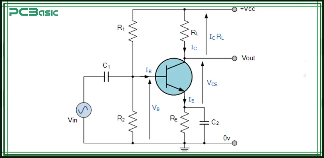
The common emitter amplifier is widely used for voltage amplification. It offers moderate input impedance, high voltage gain, and 180° phase inversion between input and output.
Operating Principle:
• The input signal is applied between the base and the emitter.
• Output is taken between the collector and emitter.
• The emitter terminal is common to both input and output.
Features:
• Significant voltage gain
• Phase inversion
• Moderate output resistance
The design is simple yet highly effective for small-signal amplification.

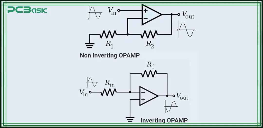
Operational amplifiers are highly versatile, enabling a range of amplification modes:
• Inverting Amplifier: Input signal is applied to the inverting terminal. Output is phase-inverted.
• Non-Inverting Amplifier: Input applied to the non-inverting terminal. No phase change.
• Differential Amplifier: Amplifies the difference between two inputs.
Characteristics:
• Extremely high open-loop gain
• High input impedance
• Low output impedance
Op-amp circuits are common in instrumentation, audio pre-amplifiers, and active filters.
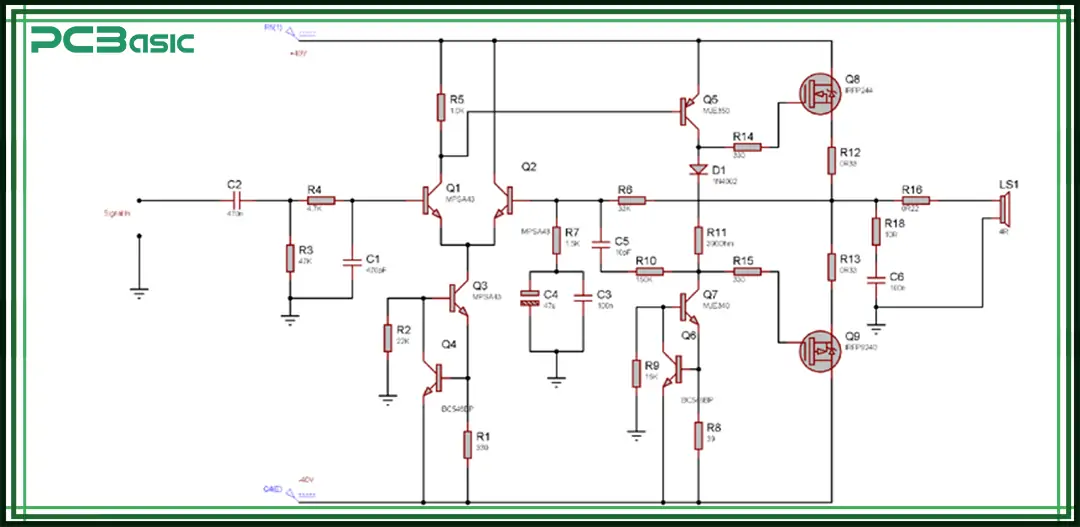
When signal strength needs to drive a significant load — such as a loudspeaker — power amplifiers are used.
Architecture:
A typical power amplifier circuit diagram shows these stages working together to ensure the input signal is sufficiently boosted and delivered with high efficiency to the load.
• The pre-amplifier stage boosts weak input signals.
• The driver stage prepares signals for power handling.
• The output stage delivers large currents to the load.
Classes:
• Class A: High linearity, low efficiency
• Class B: Higher efficiency, crossover distortion
• Class AB: Balanced compromise
• Class D: High efficiency through switching
Power amplifier circuits focus on output power, thermal management, and efficiency optimization.
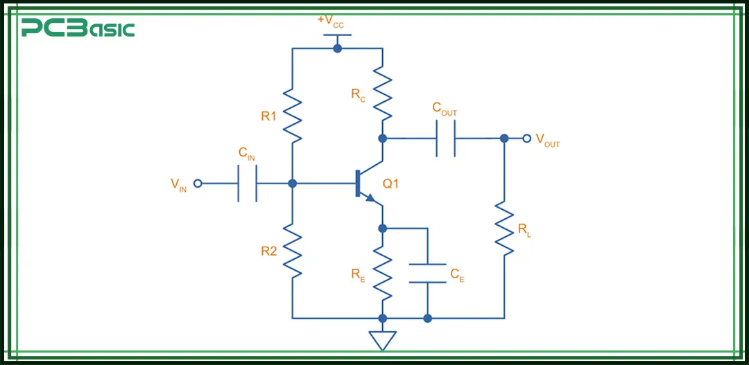
Understanding a simple transistor circuit diagram like a single-stage common-emitter amplifier helps illustrate core concepts.
Example: A single-stage common-emitter amplifier.
Here is the amplifier diagram:

Components Used:
• Transistor: NPN BJT (e.g., BC547 or 2N3904)
• Resistors: Biasing (R1, R2), Load (RC), and Emitter (RE)
• Capacitors: Input (C1), Emitter bypass (CE), and Output (C2)
• Supply: DC voltage (commonly 9V–12V)
Working Principle:
• The input AC signal passes through C1, which blocks any DC from the signal source.
• R1 and R2 form a voltage divider that biases the transistor.
• RE provides stabilization against thermal runaway.
• CE bypasses RE for AC signals, enhancing gain.
• RC acts as the load for the collector current.
• The amplified output signal flows through C2 to the next stage or load.
Design Note: Choosing values for RC, RE, and biasing resistors determines the single-stage amplifier's gain, bandwidth, and stability.
Designing an amplifier requires more than connecting parts. Several technical factors must be considered to ensure stable and predictable operation.
Temperature variations can change transistor characteristics. Proper biasing ensures that changes in beta (β) or Vbe shifts do not push the amplifier out of its operating point.
Amplifiers must maintain consistent gain across the desired frequency range. At low frequencies, coupling and bypass capacitors introduce roll-off. At high frequencies, internal transistor capacitances limit performance.
Input and output impedance matching maximizes signal transfer. For example, an audio amplifier should match its output impedance to the speaker’s input for optimal power delivery.
Higher gain usually reduces bandwidth. A designer must balance these two parameters according to application needs.
Power amplifiers generate significant heat. Heatsinks, thermal pads, or even forced-air cooling may be necessary to maintain reliability.
Sources of noise include power supply ripple, electromagnetic interference, and transistor shot noise. Shielded enclosures, bypass capacitors, and careful grounding are critical.
Positive feedback paths, unintended through PCB layout or stray capacitance, can cause oscillations. Techniques like Miller compensation are often used in high-gain amplifier designs to prevent oscillations.
Each factor must be addressed during the simulation, prototyping, and final layout stages.
Now, let’s break down the practical side of using a transistor as an amplifier. Each component plays a crucial role — and getting them right can mean the difference between a reliable circuit and a noisy, unstable one.
Function: Think of this as a security guard at the entrance. It lets the AC signal pass through while keeping any unwanted DC components out, protecting the delicate biasing inside the amplifier.
Details: Without this capacitor, the source’s DC level could disturb the transistor’s operating point. Capacitance value should be chosen to maintain low reactance at the lowest frequency of interest.
Formula:
Where:
• Xc = Capacitive reactance
• f = Frequency
• C = Capacitance
For audio applications (20 Hz–20 kHz), a capacitor in the range of 1 µF to 10 µF is typical.
Purpose: Establishes the correct base voltage and current.
Components: A voltage divider network (R1 and R2) feeds the base. The emitter resistor (RE) provides negative feedback, improving bias stability.
Important: A stable bias ensures the amplifier remains in the linear active region, avoiding cutoff and saturation during operation.
Function: Bypasses the AC signal around the emitter resistor to maximize gain.
Without CE: The AC signal develops a voltage across RE, reducing overall gain.
With CE, AC sees a low impedance path through the capacitor, effectively eliminating RE from the AC signal path.
Capacitor Sizing: Large enough to ensure low reactance at the lowest operating frequency.
Role: Similar to the input capacitor but located at the output.
Purpose: Blocks DC voltage from reaching the next stage or the load.
Effect: Only the AC part of the amplified signal is transmitted.
Value: Typically depends on the input impedance of the next stage. Lower frequencies require larger capacitance.
Working Principle: Placed in the collector circuit of the transistor. Converts variations in collector current into output voltage changes.
Selection:
• Higher RC gives higher voltage gain.
• Must balance voltage drop across RC against Vce requirements.
Formula:
Voltage Gain (Av) (ignoring RE) approximately equals:
Where re is the intrinsic emitter resistance.
Important: Selecting an RC that is too large may cause the transistor to leave the active region, leading to distortion.
An amplifier circuit diagram provides more than just a graphical layout. It represents the critical interactions between active and passive components to achieve stable signal amplification. Understanding each component’s role — from biasing resistors to coupling capacitors — is fundamental.
To achieve optimal performance, a designer must not only follow schematic guidelines but also respect real-world imperfections: temperature drifts, parasitics, and noise. In professional environments, simulation tools (such as SPICE) and prototyping are critical steps before final deployment.
Whether for small signal amplification or power delivery, mastering amplifier circuit diagrams remains an essential skill in electronics engineering.

Assembly Enquiry
Instant Quote
Phone contact

+86-755-27218592
In addition, we've prepared a Help Center. We recommend checking it before reaching out, as your question and its answer may already be clearly explained there.
Wechat Support

In addition, we've prepared a Help Center. We recommend checking it before reaching out, as your question and its answer may already be clearly explained there.
WhatsApp Support

In addition, we've prepared a Help Center. We recommend checking it before reaching out, as your question and its answer may already be clearly explained there.